This thread has been locked.

If you have a related question, please click the "Ask a related question" button in the top right corner. The newly created question will be automatically linked to this question.

ADS4149: Sampling frequency as 24mhz

Part Number: ADS4149
Other Parts Discussed in Thread: ADC3542, ADS4146

Hi, 

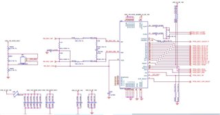
We are using ads4149. The adc input signal frequency range is 328Mhz to 335Mhz. I am planning to use 24mhz as sampling frequency, by considering the input bandwidth of 7Mhz.

For this frequency range, datasheet says 69dB as SNR expected. if I am using 24mhz as fs, will it degrade the SNR because of the undersampling? 

If yes, pls let me know what kind of impact will be there on snr and how much it may reduce because of the fold back(Alias) 

Thanks

Vetri

  • Hi Vetri, 

    We can have someone check the performance at this sample rate on an EVM in our lab, however it may take a few days to get the results to you.

    Might I suggest to look at the ADC35xx device family. These are single channel, ultra low power devices which contain an integrated NCO and down-converter. I would suggest to start with the ADC3542. You can see all of these devices by going to this link and entering "ADC35" into the search box. https://www.ti.com/data-converters/adc-circuit/high-speed/products.html 

    Regards, Chase

  • Hi Vetri,

    We had an ADS4146 on hand which is a very similar part, it is rated for 160MHz instead of 250MHz. And we were able to test it with a sampling frequency of 160MHz and 24MHz using an input frequency of 7MHz. We had filters in both the sampling frequency and the input frequency. This was to test the part at baseband, but if I am understanding correctly you want to use an input around 330MHz which would be in the 27th Nyquist?

    The results are in the attached PowerPoint, and as you can see the SNR and SFDR did not change by a lot. It actually improved by using the lower sampling frequency.

    Hopefully this answers your question.

    Best,

    Camilo

    ADS4146 160M vs 24M Fs.pptx

  • Hi Vetri,

    We repeated the test with the ADS4146, but this time with a 331MHz input frequency. The results are in the PowerPoint attached. But the SNR is definitively lower. By changing the sampling frequency from 160MHz to 24MHz we are losing around 6dBFS in SNR. By having your sampling frequency be 24MHz you are operating in the 27th Nyquist, which means you need to make sure to filter you input so that all of the noise in between your baseband and your input does not fold back into your baseband and appear in the capture.

    Reiterating what Chase said, it would be a good idea to look into the ADC35xx device family. Since these have an integrated programable NCO and down-converter.  

    Hopefully this answers your question.

    Best,

    Camilo

    ADS4146 160M vs 24M Fs 331Min.pptx

  • Dear camilo, 

    Thanks for your response. It helped me a lot. 

    Regards, 

    Vetrivel

  • No problem. Have a nice day!

    Best,

    Camilo.

  • Hi camilo, 

    I am using ADS4149 ADC in our custom board. The ADC sampling clock is driven from FPGA.

    Sampling Frequency(Fs) = 24MHz

    ADC input Signal Frequency(Fin) = 328MHz

    ADC input signal power level = -10dBm.

    FPGA Part Number : MPF200T

    I am routing the OCXO clock(24MHz) to ADC through FPGA as Fs. I could see 8MHz at the ADC output.

    Issue 1 Statement :

    Now I am generating the same 24MHz clock by FPGA's internal PLL instead of OCXO and routed to ADC as Fs. Here the ADC output itself not proper. expected is 8MHz but only junks are present.

    I have probed the ADC clock signal by oscilloscope I could make over the following difference between OCXO clock and FPGA's Internal PLL CLOCK.

    OCXO clock is varying from -0.2v to +1.5v with overshoot of 0.4v.(Attachment OCXO_as_ADC_Fs)

    Internal PLL clock is varying from -0.3v to +1.7v with overshoot of 0.5v

    From the ADC datasheet, the clock signal max voltage for LVCMOS single ended configuration is 1.8V. We are using same LVCMOS single ended configuration.

    I can see the internal PLL clock is crossing the 1.8v. Kindly let me know, the issues is happening because of this issue?

    Issue 2:

    The ADC clock is getting coupled in the ADC input signal. Fundamental is 328Mhz. Because of the ADC clock coupling we are seeing the 352MHz, 376MHz and 400MHz @23dB down from fundamental.

    Pls provide suggestion to remove this coupling issue too.

    Note: ADC Section Schematic is attached here.  ADC_input_clk_image

  • Hi Vetrivel,

    Please provide the layout of you board, gerber files would be preferred, and an FFT plot of the output so we can see the coupling.

    Regards,

    Rob

  • Hi rob, 

    Thank you for your response. We can't share those files here.So could you share your mail id. Let us discuss. It would be great helpful for us. 

    Regards, 

    Veteivel M

  • Hi Vetrivel,

    I have sent you an email so that we can take this offline.

    Best,

    Camilo