


Other Parts Discussed in Thread: TMUX1119, REF6230, , DAC11001A, OPA828
Hi Texas,
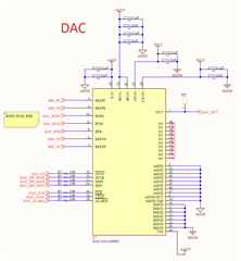
With DAC11001BPFBT I want to generate ultra-clean DC frequency bipolar buffered output voltage (-2.5 V to 2.5V) with micro-volt (say 50 uV) precision which will be further cascaded to precision analog switches (TMUX1119). I wanted to critically analyze the possible loopholes in the attached DAC design schematic for guaranteed device performance. I have the following queries:
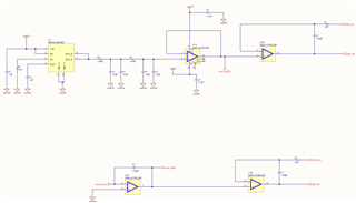
- I have used quad channel OPA4187IRUMR to design the reference section, will this arrangement (schematic attached for 3V external reference with REF6230) give any non-ideal behavior of REF_PS, REF_PF, REF_NS, REF_NF,DAC_ROFS?
- Will the DAC outperform if given the maximum possible headroom from reference supply(+/-3 V) to VCC (+10V), VSS (-10)? For minimization of noise floor should we decrease the VCC, and VSS supply?
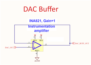
- Since DAC1101 gives unbuffered output voltage, for DC buffer output, should we use high accuracy instrumentation amplifier with Gain=1 as a buffer or precision opamp with a minimal offset voltage, ultra-low noise etc? To design non-inverting buffer (also inverting buffer ie Gain =-1) with minimum noise, offset… Could you please clarify a possible list of design parameters and parametric specifications (Offset voltage, Noise, zero drift, input bias current) that one must follow for the same?
- For mentioned requirement among e-Trim, super beta, and zero-drift opamp technology which one should be the best choice and why?
Thanks and Regards,
Deepak

