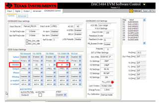
Part Number: DAC3482EVM
Hello team,
I am using DAC3482EVM with TSW1400EVM.
On the p.9 of the DAC348xEVM user's guide, it says,
Y3: FPGA Clock 1. This clock is an ac coupled LVDS. The clock rate for this should be
– FDAC/interpolation/2 for DAC3484
– FDAC/interpolation/4 for DAC3482, DAC34H84, and DAC34SH84
What does /4 mean?
Does "interpolation/4" mean that clock divider of FPGA clock on TSW1400 should be set to 4?
Best Regards,
Kei Kuwahara


