


Other Parts Discussed in Thread: THS4541, , THS4551, THS4521
Hi TI
I have looked at the Schematics for the ADC3643EVM to understand how the THS4541 is used with ADC364x in a single-ended to differential configuration. I could not find any information in the ADC366xEVM User's Guide on what components to remove or add to enable the THS4541 inputs.
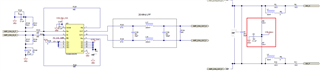
The image below is cut-out from the ADV3643EVM schematic (sbar014a.zip).
Q1: Should the components in the red box be removed when using THS4541? The FDA has already centered the differential signal at the VCM level (0.95V).
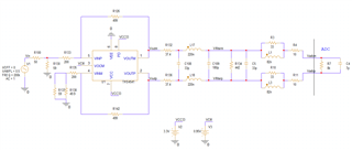
I have modelled the circuit in Pspice for TI (see image below) to get a baseline and then work from that.
Q2: I would like some sort of refence to verify my measurements in Pspice for TI. E.g. what input signal to the EVM board will give a full scale ADC input (2.25Vpp)?
Q3: Can you provide a bit of background of the EVM design? I can see the glitch filter is modified compared to suggested design in the data sheet.
Thanks, Claus

