This thread has been locked.

If you have a related question, please click the "Ask a related question" button in the top right corner. The newly created question will be automatically linked to this question.

ADS7950: The power-on sequence of the ADS7950

Part Number: ADS7950

Hi, 

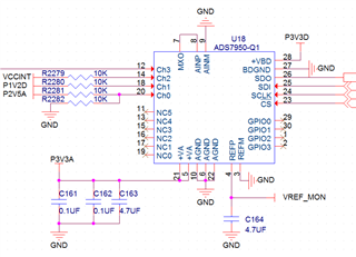
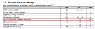
I use two pcs ADS7950 in my circuit. Under the condition that the power supply voltage of PCBA rises slowly, ADC sampling value cannot be read,nor when I rboot the FPGA on the PCBA  . I guess  that the ADC  power-on abnormally , May I ask whether it is related to the power-on time sequence of +VA,+VB and CHx? Could you please give me some relevant guidance or suggestions?

Best wish

Qi Liu

  • Qi Liu,

    1. Can you provide a scope shot of the analog and digital supplies? 
    2. The data sheet power supply section says:
      1. The devices are designed to operate from an analog supply voltage (+VA) range from 2.7 V to 5.25 V and a digital supply voltage (+VBD) range from 1.7 V to 5.25 V. Both supplies must be well regulated. The analog supply is always greater than or equal to the digital supply. A 1-µF ceramic decoupling capacitor is required at each supply pin and must be placed as close as possible to the device.
    3. Is your digital supply less than the analog?
    4. In general, it is not recommended to apply signals to any input before the supply is powered up.  From the absolute maximum condition -0.3V<V(AIN) < VA+0.3V.  This absolute max condition is what indicates that signals on the input should not be powered before the device.

    Best regards,

    Art

  • Hi  Art,

          Here is my schematic ,it seems to have two questions,

               1、no capactior is placed at the +VBD, is it necessary? What problems may  this cause?

               2、P2V5 is alreadly existing  before the supply is powered up.

    Best regards,

    Qi Liu

  • Sorry for the late response. 

    1. Yes, a capacitor is required on VBD.  You always need to decouple all supplies on all devices.  Decoupling provides a charge reservoir on the supply pin to respond to transients.  Without decoupling your performance may be impacted, and you may posibly have device malfunction.  Probably the most critical supply to bypass is a digital supply as the transients will be large and will generate noise issues without decoupling.  This video on decoupling capacitors will help you to understand the importance of this component. 
    2. Applying power to an input of an ADC, before applying it's analog and digital supplies violates the absolute maximum conditions.  This is not recommended and can result in abnormal operation or damage to the device.  In your case, you have a current limiting resistor which should help reduce the possibility of damage.  This criteria of applying the power supplies before applying signal to the input is universally true for ADC and amplifiers (this isn't specific to this particular device).  Thus, if you cannot avoid this condition, limiting the input current is a good thing to do.  Also, you could limit the input voltage using external diodes as is shown in this document: op amp protection for SAR overstress

    I hope this  is helpful to you.  Amplifier Overstress Videos  and Data Converter Overstress Videos cover these topics in detail.

    Art

  • Hi Art,

    Because of the Chinese Spring Festival, sorry for the later response.

    I have two more questions that I need your help to explain.

    1、How big is the current limiting of  protect diode which integrated into the chip input port ?

    2、What does the maximum input current in the datasheet depend on ?

    3、What  is the Vth of the  protect diode which integrated into the chip input port ? Through  Digital multimeter, the Vth from GND to CH1 is 0.76V, and the Vth from CH1 to VA is 1.57V This is why?

    Qi Liu

  • Qi,

    1.  The ESD diodes are designed for 10mA continuous current.  That is the spec that is circled in the picture above.  We do not recommend running 10mA of continuous current into the diode.  More commonly, we recomend sizing protection circuits to limit the current to 1mA to provide design margin.

    2.  The maximum input current is set by the current limiting resistance on the input, and the supply or GND that the diode is connected to.  For example, if a diode is connected to GND, and the source resistance is 1k ohm.  Driving the input to 1.3V will cause a current of approximately 1mA to flow into the input.  This is calculated as (1.3V - 0.3V)/1kohm.  The  0.3V is the diode drop.  Keep in mind that some power supplies cannot sink current.  So, if 6.4V is applied to an input where the ESD diode is connected to a 5V supply with a 1k ohm resistor, you may expect about 1mA to flow.   However, it is possible that the LDO powering the supply may not be able to sink current.  This is why you should always place a TVS diode on the supply.  This topic is covered in ADC EOS Video Seriesamplifier EOS video series

    3.  Across temperature and process the diodes are designed to start turning on at about 0.3V.  This is why the absolute maximum shows the input range from -0.3V to (Va +0.3V).  As I mention in item 2, if the Va supply is connected to an LDO this often means that the supply cannot sink current.  In this case if the input voltage is set to 6V or 7V the input signal may be routed to the supply and raise the supply above the LDO output voltage.  If the LDO output voltage is specified at 5V and the ESD structure drops 0.3V, applying 6V to the input can cause the supply to increase from 5V to 5.7V.  In cases where the supply increases, the LDO is essentially an open circuit.  This is why a TVS is recommended on the supply, even in cases where the EOS event happens on an input.  Note that your measurements seem high.  If you measure 0.7V on the diode that means it is turned on hard and you likely have more than 10mA of forward current.

    I hope this info is helpful to your.  I really recommend you watch the video series in the links above.  There is a huge amount of detail in these videos that can help you to select input components to protect your device from EOS.

    Best regards, Art

  • Hi Art,

    Thank you for your answers and suggestions

    On the third point, I'm afraid I didn't make it very clear,  I had removed the ADC chip from the PCBA before the test. If the diodes are designed to start turning on at about 0.3V. does it means this chip was damaged.

    Best wish,

    Qi

  • Zhiyao,

    If you applied a current less than 10mA through an ESD diode and it read 1.57V it is damaged.  I think that the diode test on most digital multimeters would use a current less than 10mA, so your diode is likely damaged.  If you applied a current greater than 10mA, the test itself violated the absolute maximum ratings.

    Art