This thread has been locked.

If you have a related question, please click the "Ask a related question" button in the top right corner. The newly created question will be automatically linked to this question.

ADS5296A: ADS5296A - LVDS clock driver

Part Number: ADS5296A
Other Parts Discussed in Thread: ADS4122,

Hi,

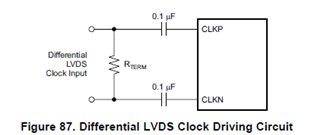
I will using LVDS clock driver to drive the clock input of the ADS5296A and ADS4122.

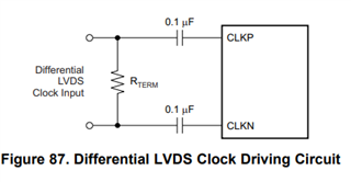
in the DS of ADS5296A I find the followed:

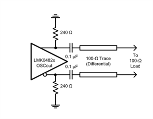
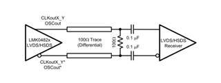
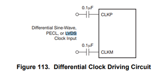
The answer to the same question for the ADS4122:

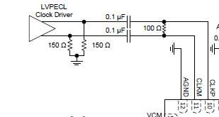
Pls. advise where to put the termination in both cases.

regards

Zeev Gerber

  • Hi Zeev,

    Thanks for reaching out to TI.

    Let me explain you why the above circuits have the termination as shown.

    LVPECL case: 

    Source Side: In order to have sufficient output swing and drive strength, the LVPECL pins needs to be biased with a resistor divider. A pull up (typically internal to device) of ~82 ohm is there and an external resistor Rterm is expected to be placed from the pin to the GND. This resistor value is typically between 120 ohm to 240 ohms. 

    Figure below shows the typical implementation. After the coupling caps, the characteristic impedance of the trace is 100 ohm, hence to avoid signal reflections, a 100 ohm termination is placed, hence the schematic looks like the one you have shared for ADS4122.

    LVDS case:

    In LVDS clocking, there should be a dc path from positive to negative terminals and the characteristic impedance is 100 ohm. Hence before the coupling capacitors, a 100 ohm termination is required.

    The same is evident in the datasheet of ADS5296A and ADS4122:

    Hence, you can place the 100 ohm termination, before the coupling capacitors when using LVDS clocks.

    For more information about the same, you can refer to section 10.4 Output Termination and Biasing in the below document

    https://www.ti.com/lit/ds/symlink/lmk04828.pdf

    Thanks & regards,
    Abhishek