This thread has been locked.

If you have a related question, please click the "Ask a related question" button in the top right corner. The newly created question will be automatically linked to this question.

ADS1262: the input of one different-input channel affect next differential chennel

Part Number: ADS1262

Hi 

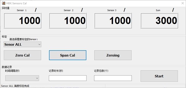
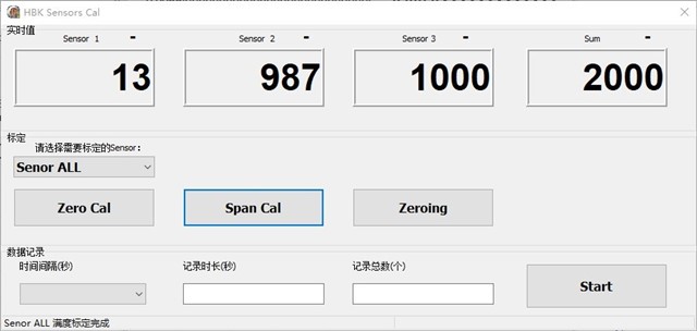
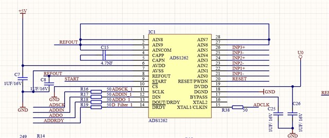
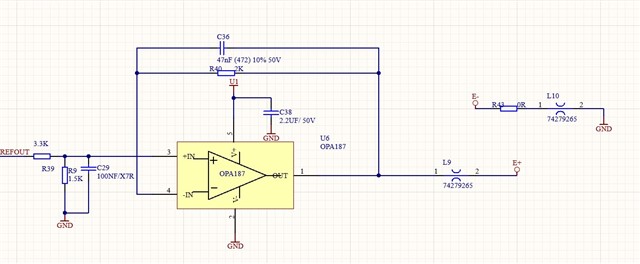
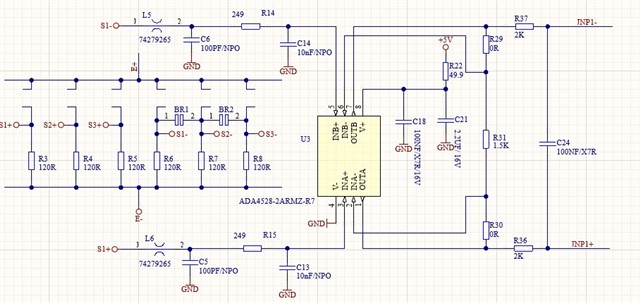
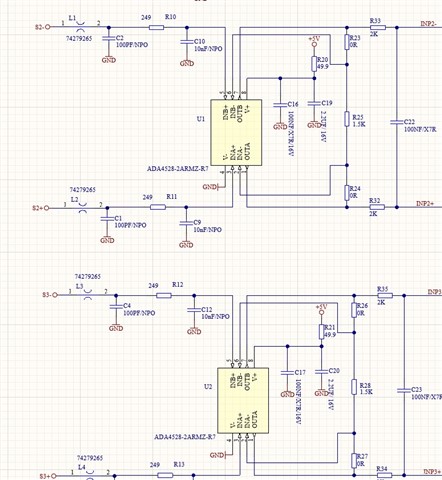
I use ADS1262 like below picture, when I change the input of one different-input channel , it will affect the output of the next differential chennel . For example, when I change the input of channel 1(AIN0,AIN1), keep the input of channel 2 (AIN2,AIN3), but the output of channel changed, I don't know why.

I want to know how to deal with this reason.

thanks and best regards

Kim

  • Hi jinyan ma,

    I am not sure I understand the issue you are having.

    It sounds like when you switch the channels, you believe the first channel is influencing the next channel - is that correct? Can you provide data that shows what you are measuring as well as the error you are seeing? It would help to know what you expect to measure on each channel, as well as what you are actually measuring on each channel

    -Bryan

  • Hi Bryan:

    What you understand is correct. we have a panel what can show the 3 sensors output .The ADS1262 collects signals of these thre e sensors'  (the SPS is1200), the gain is 32, we add FIR digital filter. we calibrated the span digital output: 1000 for this three sensors , you may see 3 sensor's output is 1000 on the panel in picture1 . when change the output for the sensor 1, the other two sensors  not change,   it is strange the output for the sensor 2 also have some change,see the picture 2.

    thanks and best regards

    Kim

  • Hi jinyan ma,

    Are all of your sensors biased at the same time? Or are you only biasing Sensor 1 and then taking a measurement, then switching the biasing to Sensor 2 and taking a measurement, then switching the biasing to Sensor 3 and then taking a measurement?

    Also, have you checked that the data from the ADC matches what you are showing in the panel? It sounds like you have additional operations being performed in your controller (you mentioned an FIR filter). Therefore I am asking if the issue could be from the calculations, or can you actually confirm that raw ADC data at DOUT is incorrect too?

    -Bryan

  • Hi Bryan:

    In my test , all the three sensors biased full scale at the same time, each sensor show it's output 1000 in the panel. when I just change the siganl for the sensor 1 from full scale to 0 , the output for sensor 1's in the panel should change from 1000 to 0, and the others should keep 1000. But now , it has two problems , 1 i: the output for sensor 1 can't  return to 0 , 2 : the output for sensor 2 can't keep 1000.

     The data from ADC match the output in the panel. FIR filter is the digital filter like the filter within  ADS1262 ,such as sinc.

    thanks and best regards

    Kim

  • Hi jinyan ma,

    This might be related to a settling issue. I see that you have a filter on the output of the op amp that has a very low cutoff frequency (~400 Hz). Can you try reducing the size of the 100nF capacitor and/or 2kohm resistors? Even reducing them to 10nF and 1kohm gives you a cutoff frequency of 7.96 kHz, which should be sufficient to reduce the settling time compared to the ADC sampling rate (1200 SPS). You could also reduce the ADC data rate to see if this has an effect on the system.

    -Bryan

  • Hi Bryan:

    Thanks for your reply . I want to know if it's necessary to  add a common filter before the input for ads1262 to remove the common noise? 

    Now the input voltage to ADS1262 is about 0.35V , the Gain for ADC is X32 , if it's OK?

    And for the Anicom pin for ADS1262, it's better to connect to REFOUT , or connect to GND?

    thanks and best regards

    Kim 

  • Hi jinyan ma,

    Here are the answers to your questions:

    I want to know if it's necessary to  add a common filter before the input for ads1262 to remove the common noise?

    Adding a common-mode filter is a good idea. You can accomplish this by adding a capacitor to ground on each analog input e.g IN2+, IN2-, etc.

    You would typically size the capacitor to be 10x smaller compared to the differential capacitor. So, if the differential capacitor is 10nF, you would choose 1nF capacitors for the common-mode components.

    Now the input voltage to ADS1262 is about 0.35V , the Gain for ADC is X32 , if it's OK?

    The maximum input signal (VIN) you can apply to the ADC is VREF / gain. The maximum VREF is AVDD + 0.1V, or ~5.3V. Both of these conditions are shown in Table 7.3.

    If VIN = 0.35V and the gain is 32, then your signal is 11.2 V, which is much greater than the ADC can support. Assuming VREF = 5V and VIN = 0.35V, then the maximum gain you can choose is 14.2. Therefore, you would need to choose a gain of 8 on the ADS1262, because the gain of 16 is too large. If your VREF voltage was smaller, you would need to choose a smaller gain as well

    And for the Anicom pin for ADS1262, it's better to connect to REFOUT , or connect to GND?

    Are you using the AINCOM pin? If you are not using the AINCOM pin, you should tie the pin to mid-supply. You can use the REFOUT pin in this case. This is described in section 10.1.7 in the ADC datasheet

    -Bryan