This thread has been locked.

If you have a related question, please click the "Ask a related question" button in the top right corner. The newly created question will be automatically linked to this question.

ADS1262: Issue with bits shifted out incorrectly

Part Number: ADS1262
Other Parts Discussed in Thread: ADS1263

I have an ads1262 with the following setup

reading differential input on ain0 and ain1 every 10

400sps

gain 16

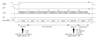
CRC and status byte enabled

1 out of about every 12000 reads (about every 2 minutes) I get a reading where the bits are all shifted left 1. This is very odd and will still pass the CRC test, along with messing up my system because of the bad read being double what the last one was.

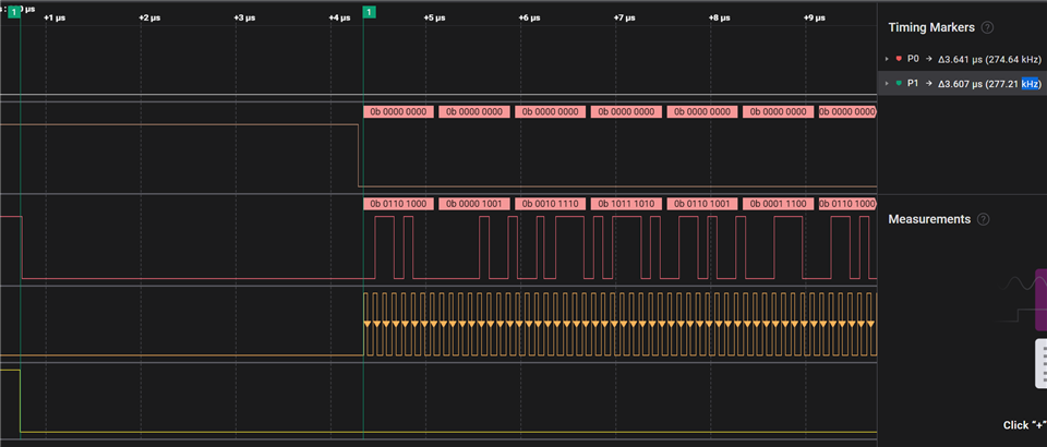
The above image is the read right before a bad read. (top to bottom MOSI, MISO, CLK, CS)


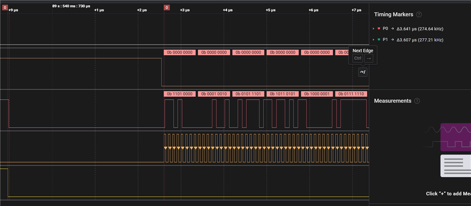
This image reading is roughly 10 ms after the reading above it. As you can see all of the bits are shifted over to the left one. I am able now to use the Status bit to show that it's a bad read since I don't have an ads1263 the 8th bit should always be 0, also I'm using an external clock so the 6th bit should be 1. I've found how to hopefully not let this affect my system. I'm curious is this a common problem(it happens on the 6 prototype boards I have)  What can I do to fix this? It happens at all clock frequencies, it is much more prevalent at lower speeds 1 MHz. Currently, I run at 10 MHz.  My signals look very clean so I'm looking for some advice. 

  • Hi William Dunkley,

    In the top image, you show 7 bytes being clocked out. However, I would have expected only 6: STATUS, 4x data bytes, CRC. The 7th byte is the same as the 1st byte. Are you repeating data then with the additional clocks?

    How do you know when new data is ready to be clocked out - I don't see the DRDY pin in your logic analyzer captures. Are you using the ADC1 bit in the STATUS byte?

    The system clock (CLKIN) and serial clock (SCLK) can be a maximum of 8 MHz. You mentioned that are using 10 MHz, but I'm not sure which clock that was for. In the images above, I counted 10 clock periods within 1 us, so this implies you are running SCLK at 10 MHz, which is not allowed. Please see table 7.3 and 7.6 for more information

    -Bryan

  • I apologize for the confusion by adding the extra byte in the image. I am currently reading all the bytes 3 times and comparing them, this was an attempt to catch bad readings.

    We are not using the DRDY pin, nor am I looking at the ADC1 bit. I could easily look at the ADC1 bit.

    As for the Speed, I didn't try 8 MHz. However at 1 MHz and 5 MHz, I got 10+ x  more errors at 1 Mhz than I did at 10 MHz which is why I went with that speed. I also got more errors at 5Mhz, but it was less than 1MHz. Do you have any idea why a slower speed would result in worse readings? 

  • Hi William Dunkley,

    Just to clarify, which clock(s) are being set at 10 MHz (or 1 MHz, 5 MHz, etc.) ? Is that both SCLK and CLKIN? Or just one or the other?

    -Bryan

  • The CLKIN is a 7.68 MHz crystal, and the clock I've been referencing is the SCLK. 

  • Hi William Dunkley,

    I see in your original post you said you are converting continuously between AIN0 and AIN1. You also said "every 10", but it was not clear if that was microseconds, or some other interval. Can you please confirm?

    And how are you deciding when to clock out data then if you are not using DRDY or the ADC1 bit in the STATUS byte? Are you just using a timer?

    If you want to send a .sal file showing the logic analyzer capture over multiple sampling periods, please do so. This might be easier to review compared to screenshots.

    -Bryan

  • In the future, we will Multiplex through different channels. But currently, we are only reading the first differential port, although it does look like we set the port each time. 
    We just read it every 10 ms based on a timer.ADS1262 Capture.zip 

  • Hi William Dunkley,

    If you are sampling at 400 SPS (2.5 ms), why are clocking out data every 10 ms - won't you miss a few data samples?

    My guess as to what is happening here is that your timer and the ADC are getting out of sync over time, and you are starting to read data during the "quiet period" (see Table 9-17 in the datasheet). It makes sense then why you see more errors when SCLK is slower, because the time to clock out data (6 bytes) is longer when SCLK is slower. This increases the probability that you will start clocking out data during the quiet period.

    I would encourage you to instead use some sort of interrupt to identify when you should read data. As mentioned previously, you can use the dedicated DRDY pin, you can poll the ADC1 bit in the STATUS byte, or you can use the combined DOUT/DRDY pin for this functionality (see section 9.4.4.4 for more info on how this pin behaves). When the DRDY pin transitions from high to low (or ADC1 bit transitions from 0 to 1) you can begin clocking out data.

    Please try one of these methods and see if the issue goes away. I would also encourage you to use an SCLK speed as specified in Table 7.6

    -Bryan

  • Thanks Bryan, I'll give the DRDY pin a shot as I did connect it to something on my board. I'll update this thread with the results. 

  • This worked great, using the DRDY pin got rid of all the CRC failures and Shifted bits issues that I saw.  It does seem like the software version of checking if new data is ready has some issues as I would always see a 1 for new ADC1 data but would sometimes get bad data. Thanks so much for your help Bryan. 

  • Hi William Dunkley,

    I am glad this issue was resolved without too much effort. If you have additional questions, please start a new thread and we will support you there.

    -Bryan