This thread has been locked.

If you have a related question, please click the "Ask a related question" button in the top right corner. The newly created question will be automatically linked to this question.

ADC32RF55EVM: CMFB circuit in ADC32RF54EVM

Part Number: ADC32RF55EVM
Other Parts Discussed in Thread: ADC32RF54, OPA376, LMH5401

Hi,

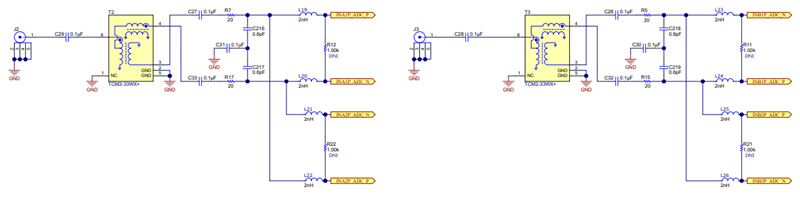
In the evaluation board of the ADC32RF54 there is a CMFB made of OPA376.
If I understand it right, the purpose of this circuit is to reduce the CM error of the ADC driver (LMH5401).

The weird thing is that the LMH5401 already contains internal CMFB circuit which serves the same purpose.
Why did we need another external circuit that is doing the same thing?
Do you have any explanation?
LMH5401 internal CMFB circuit

Thanks

  • Hi Sagi,

    The OPA376 was used chosen prototyping stage of development and was to ensure the best performance and functionality when using multiple LMH devices (as we were not fully sure on the output CM ability of the ADC - ie it's ability to drive the internal CMFBs). Using this external device was simply a safety measure of ours during initial prototyping. You should be fine to use the internal CMFB buffers of the LMH amps without any additional op amp as on the EVM.

    On this ADC32RF5x + LMH5401 EVM design, you will find we actually have 4 separate input networks. This is so we could validate quad channel ADC devices of this family in the future as the pinout will be pin-to-pin compatible. Please note that if you are planning to use ADC32RF5x (dual channel device) in a 4x averaging mode, then we recommend to split the input into the Ain1 and Ain2 as shown in the datasheet in Figure 8-8. This would be repeated for channel B as well, and only 2 LMH5401 will be required. Instead of the TCM2-33WX+ baluns below, simply replace this network with the amplifier network. The split should remain as in the schematic below.


    Thanks, Chase