This thread has been locked.

If you have a related question, please click the "Ask a related question" button in the top right corner. The newly created question will be automatically linked to this question.

ADS124S06: Acquisition Problem

Part Number: ADS124S06

Hello,

Sorry for this silly question, but I have to admit that I can't figure it out.

I use a sensor powered by 3V3 which has two analog outputs. These outputs have a reference which equals VDD/2 with respect to ground. I will call this reference the "negative" pole.
These two analog outputs can therefore vary from -1V25 to +1V25.

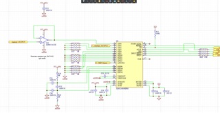
I was think easy for me to connect it to the ADC ADS124S06. I connected the negative pole to the AINCOM input and the + poles to AIN0 and AIN1. I use as an external reference the 3V3.

For information, here is the schema of this part.


In the software I have configured the following registers:

DATARATE: 0x38 //configure 200SPS, low-latency filter, single shot
REF: 0x30 //configure REFP_BUF and REFN_BUF disabled
VBIAS: 0x00
PGA: 0xC8 //configure PGA enabled, conversion delay 4096*tMOD
For my test in the INPMUX register: AINCOM is configured as negative input and AIN1 as positive input

The others registers are left with the original values.

I don't know what I did wrong, but it doesn't work properly.

To do a test I use a lab power supply where I place AINCOM on the - terminal and AIN1 on the + terminal. What is strange in this configuration the value of the ADC remains constantly close to value. If I place AINCOM on the + terminal and AIN1 on the - terminal, that gives me a correct negative value and I can go up to 3V25?!

If I change the PGA configuration to 0xC0 (PGA bypassed):
To do a test I use a lab power supply where I place AINCOM on the - terminal and AIN1 on the + terminal. In this configuration the ADC value is correct up to around 0V3 with a positive value, beyond that the value is no longer correct. If I place AINCOM on the + terminal and AIN1 on the - terminal, that gives me a correct negative value and I can go as far as 3V3?!

Can you give me some clues please?
THANKS.

  • Hi Hendrickx Olivier,

    One thing I noticed in the schematic snippet is you show two different ground symbols where the AGND differs from digital ground symbol.  The grounds should be at the same reference point.  Generally a common ground is preferred, but a star ground configuration would also work.  The key consideration here is the AGND and DGND should not vary by more than 300mV apart when using unipolar power supplies (AVSS is connected to AGND).  Any trace or device inductance can cause issues if transients are present.

    I also see that there is no antialiasing or input protection to the ADC.  Connecting a bench supply directly to the ADC can be an issue that if the current through the device exceeds 10mA the ADC can be damaged as per Absolute Maximum Ratings.

    As to the issue you are seeing, you are testing the circuit differently than what was intended by your design.  You are also assuming that the bench supply you are using is within the input range of the ADC.  I have often seen AC powered bench supplies differ relative to earth ground by 40V or more.  So this means you really need to have a common ground point.  If the output voltage of the bench supplies relative to AGND is outside the input range of the ADC, then you again you are exceeding the Absolute Maximum Ratings of the ADC and can damage the ADC.

    So I would suggest using an equal value voltage divider (10k for example) for AINCOM where the resistors are connected between 3.3V and AGND and the junction of the resistors connected to AINCOM.  The bench supply can be connected with the - terminal connected to AGND and the + terminal connected to AIN1.  This is called a pseudo-differential measurement where you will see positive codes above 1.65V (3.3V AVDD/Ref) and negative codes below 1.65V when the voltage is connected to AIN1.

    Best regards,

    Bob B

  • Hi Bob,

    First, thank you for your quick response.

    Regarding the ground symbols in my diagram, it is not on this part of the diagram, but all the grounds are electrically the same, they meet at the same point on the PCB.

    You are right there is no antialiasing filter or protection. For the future do you have a few things to offer?

    Thank you for suggesting a test procedure. You were right, the ADC was HS with my previous manipulations. I placed a new one. I hope when I connect my sensor that it will work. In the meantime, I will use this setup to finish my software.

    Best regards

    Olivier

  • Hi Olivier,

    As far as input protection there are two primary concerns but they are both related.  The first concern relates to input voltage.  The Absolute Maximum Rating for the analog input voltage is 300mV from the analog supply rails.  Beyond 300mV the ESD diodes will begin to conduct.  The second concern relates to the Absolute Maximum Rating for the input current.  It the input voltage exceeds the input range, the ESD diodes will conduct and current will flow through the input pins.  This current must be less than 10mA maximum.

    As to the amount of protection required will depend on the system.  For example, if the sensor has wiring connected to the ADC, the wiring can pick up EMI/RFI which can produce a transient that may exceed the supply voltage and current could potentially flow through the input pins.  The amount of protection required in this use case would be much different than an onboard sensor that is PCB trace connected and not exposed to an outside the system environment.  You can see an example for prevention of electrical overstress in this application note.

    In your circuit, the current can be limited as a part of the antialiasing filter.  There is a discussion on the input filtering in section 10.1.2 on page 87 of the ADS124S06 datasheet.

    Best regards,

    Bob B

  • Hi Bob,

    Thank you for these suggestions. I'll look at it more closely.

    Thanks again for your help.

    Good day

    Olivier