This thread has been locked.

If you have a related question, please click the "Ask a related question" button in the top right corner. The newly created question will be automatically linked to this question.

ADS1262: What does the ADS1262 require to achieve a 25-bit noise-free bit?

Part Number: ADS1262

I am using the ADS1262 for high precision acquisition, the reference voltage is using the ADR4550, and the test signal source is using a 18650 lithium battery(4V ). Using the highest 2.5SPS sin4 mode, the code noise is about 21~22-bit stable. If you switch directly to AVDD + AVSS, the data noise can be about 23~24bit.

When using the reference voltage, 1k+10uF is used for RC filtering to reduce the reference input noise. (The voltage drop caused by the 10K resistor is ignored for now.) The signal is increased from 21~22bit to about 23bit. It shows that the reference voltage still contributes a lot to the code noise

As seen in the datasheet, up to 25 bits can be achieved (Noise Free Bits)。I want to know whether this parameter is conservative or theoretical. To achieve this performance, how low should the reference voltage noise  and input noise be  (? uVpp)

The reference layer only makes all-copper into the AGND and ensures that no current flows on it (except for the signal input capacitor filter current)
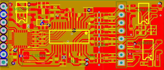
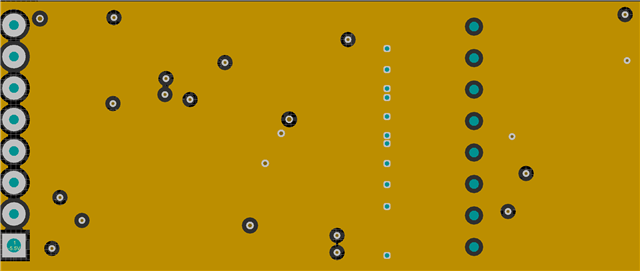
I want to get the nominal 25bit(The reading is noise-free), whether I can do it, I need to do those optimizations

  • Hi minhua chen,

    Achieving a system with 25-bit noise-free resolution is very difficult. The noise in the datasheet is reported with inputs shorted, which means the input voltage is 0 (VIN = 0V) and there is no reference noise being added to the system (because VIN = 0V). You can refer to the "ADC noise" videos in our TI Precision Labs training content to learn more about why these statements are true: https://www.ti.com/video/series/analog-to-digital-converters-adcs.html

    Once you actually start applying input signals, you will add noise to the system that will begin to degrade performance. This is unavoidable e.g. the 1k resistor in the reference path has a thermal noise of ~3-4nVRMS

     Also, effective resolution and noise-free bits (Table 8-2 in the ADS1262 datasheet) assume that the entire ADC full-scale range is being used. So if VREF = 5V, then the FSR for the ADS1262 is +/-VREF/gain, which in your case is +/-5V. If your input signal range is 0-4V, then you are using <half of the ADC's FSR, which means you are losing >1 bit of resolution simply by not using the ADC's entire FSR. You can refer to the link above for more information about this topic as well.

    Therefore, given your system settings, it seems like you are getting the best possible performance if you can get 23-24 bits noise-free

    -Bryan

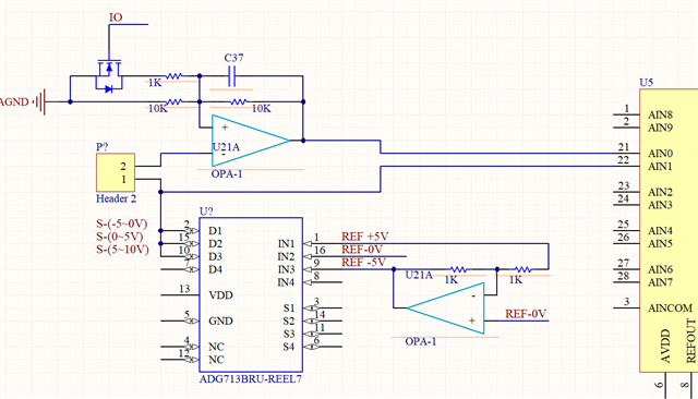
  • Thanks for the idea, I have some ideas about using ±5V, see if there are any flaws?

  • Hi minhua chen,

    Please note that the ADC full-scale range (FSR) is +/-5V, assuming VREF = 5V and gain = 1. However, this refers to the differential input voltage, not the absolute input voltage. For example, if you set AINP = AIN0 = 5V and AINN = AIN1 = 0V, then the ADC will measure AINP-AINN = 5V. However, if you switch those voltages such that AINP = AIN0 = 0V and AINN = AIN1 = 5V, then the ADC will measure AINP - AINN = -5V. Note how both voltages in this case are >=0V i.e. they are not negative. Only the differential voltage is negative. So I don't think you need to add all of this circuitry to generate negative voltage using inverting op amps.

    I would strongly encourage you to review the ADC noise information I linked to in my previous post. There seems to be a misunderstanding regarding what the ADC datasheet noise info actually represents

    -Bryan