Hi there,
I am using the ADC128S102WGRQV. In the part datasheet in section 7.3.2 it is recommended to keep the input resistance to <100 Ohm. However with such a low external resistor value we won't be able to limit the ADC internal ESD diode current to less than 10mA (our ADC driver output voltage can exceed the ADC Vref).
So I need to increase the size of the external input resistor to more than 100 Ohm and so if possible I would like a clarification on the 100 Ohm recommendation. I am trying to find more info on that recommendation.
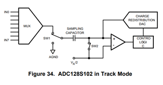
From the datasheet section 7.4.1 I understand that the track mode lasts for 3 clock cycles and the other side of the sampling capacitor is Vref/2. The sampling capacitor is 30pF (section 7.3.2) and Rmux about 500Ohm.
From my view, please let me know if correct: as long the RC formed by the external input resistance (+Rmux) charges the sampling capacitor (30pF) to within 1 LSB of the max input voltage in the 3 clock cycles, then the input resistance makes no difference (as Csample is charged). In other words: is it true I can make Rinput as big as I like as long as I consider the charging time in 3 clock cycle?
As an example:
given that the ADC max clock frequency is 16MHz, the ADC minimum sampling time would be 187ns (3 clk).
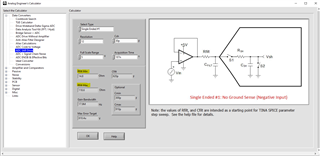
Assuming Vref=5V, then the maximum voltage on sampling capacitor is 2.5V. Even with Rext=300Ohm (800 Ohm total including Rmux) the sampling capacitor is charged to within 1LSB of 2.5V in 187ns.
So I am not too sure where the 100Ohm recommendation comes from.
Also note: by putting a capacitor at the input I have extra charge that is only limited by Rmux, so the calculations above are conservative because the assume all the charge needed to charge the sampling capacitor comes from the ADC driver.
Does anybody know Is there something else I should taking into account? Or can I increase the external input resistance as long as I make sure the Csampling is fully charged (within 1LSB) during the sampling phase?


