This thread has been locked.

If you have a related question, please click the "Ask a related question" button in the top right corner. The newly created question will be automatically linked to this question.

ADS8881: in the dasy-chain mode, the interface timeing diagram seem to be wrong (Figure 61 datasheet)

Part Number: ADS8881
Other Parts Discussed in Thread: ADS8883

the ADS8881 has different modes. i wanted to use the "10.4.2.1 Daisy-Chain Mode Without a Busy Indicator" because it seems to be the easiest if You only want to connect one device per SPi-interface. there are only 3 signals used. and in the diagram "Figure 61. Interface Timing Diagram: For Two Devices in Daisy-Chain Mode" there is exactly 18 SCLK cycles used per device. i only have one device and would need 18 cycles. the problem is: the ADC gives me only 13 data bits. i have to add five additional clock cycles to get all the 18bits out.
the strange thing is: all SPi-modes whit DiN as chip select have some additional 5 SCLK cycles in the diagrams (Figure 53. Interface Timing Diagram: 3-Wire CS Mode With a Busy Indicator (DIN = 1) as example).

now i wonder: should i clock 18+5 cycles per ADC in the dasy-chain mode? or should i add some 5 clocks in the "converting time"? what is the reason of the 5 extra clocks in the SPi-modes?ads8881.pdf

help!!!
  • Hello Oliver,

    Thank you for your post.

    I think the figures you are referencing are misleading. I interpret them as suggesting SCLK can be in one of the following states: idle high, idle low, or toggling. In any case, SCLK should be ignored by the interface until CONVST goes low.

    Please refer to Figure 50, which shows a connection diagram for 3-wire interface for a single ADC device. DIN should be held high to DVDD (not low - that is only for daisy-chain mode).

    Regards,

    Ryan

  • thanks

    i can also try the 3 sire interface. but im still wondering, why the dasy-chain isnt working as expected. do You have an idea what could be wrong?

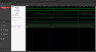
  • also i changed to the 3 wire SPi no busy "Figure 51. Interface Timing Diagram: 3-Wire CS Mode (DIN = 1)", and its the same: if i use 18 sclk's then i only get 13 data bits, if i use 18+5 sclks i get the full 18 bit data. whats the problem?

  • Hi Oliver,

    I think the data capture you shared above is pretty clear. Let me ask some colleagues about this behavior and get back to you. I'm wondering if SCLK is actually required to have 5 high-low or low-high transitions while CONVST is high for some reason. I don't see it mentioned explicitly anywhere in the data sheet either.

    Regards,

    Ryan

  • could it be that everybody uses some MCU whit an SPi interface that transfers 3x8 bits... then there would only be a question about how much You have to shift the output word, but it would work anyway.
    and about the question if the SPi-mode or the dasy-chain-mode is better for my applikation: its the dasy-chain, because it doesnt use a high-Z-state at DOUT

  • i found the problem: there are ADS8883 populated on the board instead of the ADS8881 - sorry...

  • No worries, Oliver. Glad you figured it out. Slight smile

    Regards,

    Ryan