This thread has been locked.

If you have a related question, please click the "Ask a related question" button in the top right corner. The newly created question will be automatically linked to this question.

ADS131B04-Q1: Erroneous data readings by the ADC converter.

Part Number: ADS131B04-Q1


Hello,

In our project, we are using the ADC mentioned in the subject of the question. The converter seems to be measuring the input voltage incorrectly. During our tests, I performed two voltage measurements.

The first measurement was taken by applying a voltage of 160mV to CH0P input, with CH0N connected to AGND. The obtained voltage was 159.565 mV. For a test voltage close to 1.2V, the error is approximately 4mV, which is not acceptable to us.I would like to add that the supply voltage to the ADC is adequately filtered, and the measured voltage has been verified using an oscilloscope and a METRAHIT meter.

Moreover, I used the internal calibration feature, which disconnects the measurement circuit and sets the voltage Vref = 160mV for a gain of G=1. The measured voltage was 152.15 mV.

What is the reason for such a difference in the measured voltages? How can I properly calibrate the voltage readings so that the error approaches the one specified in the documentation?

Below, I am sending the ADC connection diagram and the bit response from the ADC on the logic analyzer( Change the file extension to .sal and open the workspace in the Salae software ).


I read the voltage value from the register, and the falls within the range of 0-8388607.
Here's the formula used to obtain the voltage from ADC step:

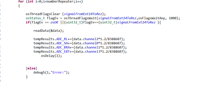
 Session.csvSession2.csv

  • Hello Kamil,

    welcome to our e2e forum and thanks a lot for your interest in our ADS131B04-Q1.

    I didn't review your logic analyzer plot and the code example yet, as it seems like you can properly communicate with the device and read data.

    Your schematic looks good also. Just pay attention to the inductance in the supply paths. Some ADCs draw quite a bit of current during power-up which can cause the supply to droop due to the voltage drop created across the inductor. In those cases the device might not power up properly. I have not seen such issues with the ADS131B04-Q1 yet though. But it might be a good idea to probe the voltages once at the AVDD and DVDD pins during power up to be safe.

    The measurement "inaccuracy" you are experiencing seems to be within specification.
    Without any calibration the device has an initial gain error of 0.2% (typ) / 0.7% (max). So for a 1.2V input signal you can expect an error between 2.4mV and 8.4mV.
    The internal test signal cannot be used to calibrate the gain error unfortunately. I assume that is what you tried to do when you say "I used the internal calibration feature, which disconnects the measurement circuit and sets the voltage Vref = 160mV for a gain of G=1."
    In order to calibrate the gain error you would have to apply a precision test voltage externally and then calculate the gain error compensation value based on the ratio between measured and applied value.

    Perform an offset calibration, before running the gain calibration, by shorting the inputs internally (or better - if feasible - externally) and averaging multiple readings. To short the inputs internally, set MUX0[1:0] = 01b.

    Regards,
    Joachim Wuerker

  • Thank you for your response.

    Unfortunately, during ADC offset calibration, I do not have the option of externally connecting to AGND. The only possibility is internal ADC offset calibration through its MUX converter. The offset is measured on channels 0 and 2.

    I have two measurement options - the first when the measurement voltage is applied to the ADC input pins, and the second when the measurement voltage is turned off, so the pins are in a float state. In both cases, MUX0[1:0] = 01b. Which way of reading the converter offset is correct?

  • Hello Kamil,

    ideally you would perform the offset calibration on all ADC channels where measurement accuracy is important to you. The offset error can be different on the various channels.
    Using the internal Mux short connection option for offset calibration is sufficient for most customers.

    It doesn't really matter which of the two options you use. When you set MUX0[1:0] = 01b, the analog inputs are internally disconnected from the ADC inputs and the ADC inputs are shorted to GND. See figure 8-2 in the datasheet for more details.

    Regards,
    Joachim Wuerker

  • Hello Joachim,

    I mentioned the two offset calibration methods because depending on which method I choose, I get different results. If I apply a voltage to the converter pins, it reads an offset voltage Voff ~ 1mV on channel 0 and Voff = 0.5mV on channel 2. For the voltage-unapplied method, the values obtained are Voff = -0.2mV on channel 1 and Voff = 0.11mV on channel 2, so there is a significant difference in the readings. Therefore, my question is, which value can be considered correct?

  • Hello Kamil,

    that is very interesting. In theory it shouldn't matter, because we disconnect the external analog inputs from the ADC when we short the inputs internally. Maybe there is some sort of coupling going on.

    Did you average multiple readings to derive the offset value? You should probably also discard the first three readings after you shorted the inputs internally because the digital filter needs time to settle.

    I would probably run the calibration with the external signal connected then, because that is closer to how the device will be used eventually.

    Regards,
    Joachim Wuerker