This thread has been locked.

If you have a related question, please click the "Ask a related question" button in the top right corner. The newly created question will be automatically linked to this question.

ADS6145: Unused CLKOUTM pins in CMOS mode.

Guru 12185 points
Part Number: ADS6145
Other Parts Discussed in Thread: LMX2820, LMX2592, LMX2572

Hi,

When used only in CMOS mode without LVDS mode, the CLKOUTM pin assumes the role of OVR. Is it okay to leave the CLKOUTM pin open if I am not using it?

It is also recommended that the CLKP pin be AC-coupled with a capacitor for input. In that case, could it be a problem that a damping resistor is inserted before the capacitor?

Thanks,

  • Conor,

    You can leave the OVR output floating if not used. There can be some resistance before the AC coupling capacitor but I would suggest to keep any series resistance under 20 ohm. If you provide us with the front end schematics then we can review further and get more feedback to you. 

    Regards, Chase

  • Hi Chase,

    There can be some resistance before the AC coupling capacitor but I would suggest to keep any series resistance under 20 ohm.

    Is it better to place a damping resistor from the perspective of noise countermeasures? Or is there a possibility that it will have a negative effect? The clock is 80MHz. The connection is input from the FPGA to pin 7 of the ADS6145IRHBT via a coupling capacitor.

    Similarly, please insert a damping resistor for the output signal from the ADC and check if there is a problem. This connection is also currently connected directly from the ADC to the FPGA.
    ・Output signal from CLJOUT_P pin
    ・D0~D13 signal

    Thanks,

    Conor

  • Hi Conor,

    If there is a pad in front of the ADC, then this will help combat standing waves. A single series resistor will not do anything except act as a low pass filter with regards to the trace capacitance. FPGA to clock the device is undesirable due to their poor jitter performance. A pad will not assist with that at all, and if anything, will reduce slew rate and increase aperture jitter on the ADC. I would suggest a straight connection with an AC coupling cap for the clock input.

    Regarding the output terminations, in CMOS mode, you should add a series resistance to prevent charging the output trace. I would suggest to start at 150 ohm. At 80MHz sample clock in CMOS mode, the output will update at 80MHz because CMOS mode uses single data rate (one sample per full clock period), this is equal to 1/(80MHz) = 12.5ns. In this document, you can see the effect of increasing the series resistance on both the voltage and current waveform on page 4. Remember that you are looking at a 12.5ns window for settling. Also, this plot is for a fixed 5pF load capacitance. This device can support up to 10pF load capacitance on each output trace. If at the worst case of 10pF, then the RC will double, so we would expect the 6ns of settling time with a 150ohm trace at 5pF to change to 12ns of settling time. This is sufficient as you are within 12.5ns. To make the settling faster, reduce this 150 ohm load to 100ohm and it will change to 8ns, but this means higher current as the device is now driving a lighter load, so expect power consumption to rise.

    https://www.ti.com/lit/an/sbaa486/sbaa486.pdf 

    Regards, Chase

  • Hi Chase,

    Thank you for your reply.

    FPGA to clock the device is undesirable due to their poor jitter performance.

    We are using 4 ADCs in parallel and are controlling the ADCs using an interleave method by shifting the clock phase by 90 degrees, but is there any recommended method other than supplying the clock from the FPGA?

    Thanks,

    Conor

  • Hi Conor,

    I'm not sure I understand what exactly you are asking about? Can you rephrase and ask again?

    Regards, Chase

  • Hi Chase,

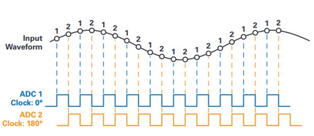
    The image of interlib ADC is as below.


    The photo above is an example of interleaving with two ADCs, but what we are trying to implement this time is four ADCs. Control is performed by shifting the phase by 90 degrees using FPGA. You say that it is not desirable to supply the clock from the FPGA to the ADC, so I would like to know what alternatives there are.

    Thanks,

    Conor

  • Hi Conor, 

    Clock synthesizer will achieve much better performance than using FPGA as a clock. FPGA clocks are known for their poor phase noise and jitter performance where dedicated clock synthesizers are designed and intended for use cases such as clocking ADC or DAC. Such as LMX2572, LMX2592, LMX2820, etc. 

    Thanks, Chase

  • Clocking with FPGA will work but you will not achieve datasheet performance from the ADC.

  • Hi Chase,

    Clock synthesizer will achieve much better performance than using FPGA as a clock.

    Is it possible to achieve interleaving similarly by not using a clock synthesizer, but by using the input of each ADC as an input from a crystal oscillator, and controlling the oscillator's enable pin with the FPGA?

    Thanks,

    Conor

  • Conor,

    If the crystal oscillator has a deterministic phase relationship upon startup and the FPGA is capable of starting the crystal oscillator within the required time, then yes it would work. I don't know of any crystal oscillator that is capable of starting at the same point of the sine wave however so this is highly unlikely to be a solution. An analog time dely and or phase shift is what should be used for this application. TI does not sell any kind of 90deg hybrid coupler however so you will have to look elsewhere.

    Regards, Chase