This thread has been locked.

If you have a related question, please click the "Ask a related question" button in the top right corner. The newly created question will be automatically linked to this question.

DAC53202: Whether it can be used to regulate the negative power supply?

Part Number: DAC53202

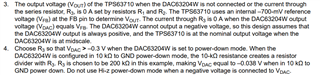
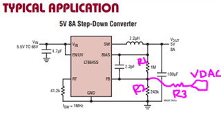
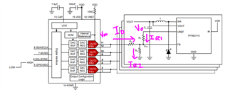
    For a DC/DC circuit that outputs negative voltage, is it feasible to adjust the negative rail by changing the magnitude of the current from the source current of the DAC and passing it through the resistor between FB and VOUT, and finally injecting it into the negative rail?

    The output of the DAC is generally about -1V relative to GND, does this violate the compliance voltage requirement of the DAC?

  • Hello, 

    Yes this is feasible. Here is an app note that discusses how to use this device in this application:

    Negative Voltage Margining and Scaling Circuit With Voltage Output Smart DAC

    The output of the DAC should never see a negative voltage, so the series resistance should be sized accordingly so the DAC does not see a negative voltage even in power down mode: 

    Please review the app note and let me know if you have any more questions. 

    Best,

    Katlynne Jones 

  • Hi,Katlynne:

        Thanks for your many helps, I'm going to switch to Vout to continue experimenting.

        Another problem is that I set the power-on reset state of the DAC53202 to Hiz, and connect it to a DC/DC FB with a positive output voltage through a 50ohm resistor. The circuit worked fine until this resistor was soldered (it could output the voltage I wanted). However, after soldering this resistor, the DC/DC is damaged at the moment of power-on. I'm sure it was because the DAC was connected that caused the damage.

        The same scenario that caused damage was when I set the power-on reset state of the DAC to Iout.

        The damage appears to be overcurrent or overvoltage, but a simple external measurement can conclude that the MOSFET inside the DC/DC controller has been broken down, and the controller is short-circuited to GND on both the VIN and SWO pins.

         The DC/DC used in this case is the LT8645s and yesterday it was the LT8361.

    Best,

    Lin

  • Hi Lin, 

    You will need to use a series resistor larger than 50Ω. What resistance are you using for the R1 and R2 resistors on the LT devices? And to confirm, are you connecting the 50Ω resistor where I have R3 shown in this diagram?


    For example, if you are using the resistances in the example figure from the LT datasheet, the nominal current through R1 and R2 is 4uA. The DAC leakage in hi-z mode with the 50Ω resistance could be larger than the nominal 4uA, which causes more current to flow through R1 and the output of the DCDC to rise. If this leakage is very large then the DCDC output could rise to an unsafe level. Or, there could be a power-on glitch on the DAC output when the system is powered on and the 50Ω resistance is causing a high current spike across R1 that could be causing the DCDC output to rise to an unsafe level. . 

    This could be a similar issue you facing in IOUT mode as well. If you are using the 250uA range this is much larger than the nominal 4uA. Setting the IOUT to sink 250uA would cause the total current through R1 to be 254uA. With a 1MΩ resistor this would set the DCDC output to 250V which is too high based on the LT8645 datasheet. 

    Best,

    Katlynne Jones

  • Hi Katlynne,

        According to the doc, when Vout is set to -5V, R1 and R2 are 1meg and 243k, respectively, then R3 is about 881k.

        Within the compliance range of Vout, the adjustable current is 0~(VDAC-VFB)/R3(A), which is only about 3uA. That is, I can adjust Vout to -8V at most, and I want to be able to adjust it to -50V, it seems that I need to add a level of amplification circuitry!

    Best,

    Lin 

  • Hi Katlynne,

        The 50ohm resistor started with 4.99K. But I guess that might not be critical, because DAC53202 is in high impedance output mode and its Ileak is typically 10nA.

        Maybe I forgot to initialize DACx-data, maybe it's a reason, I set the range of 50uA, then the reset state is -50uA, and the voltage will be increased by 50V through R1, but this doesn't seem to exceed the withstand voltage of the MOSFET.

        Another anomaly is that the enable signal of the LT circuit is high before the FPGA is configured, then it is programmed low by the FPGA for a period of time, and finally it goes up again (because the register query of the DAC shows that it can be powered up). What I want is that the LT circuit should be disabled until the DAC registers are verified.

    Best,

    Lin

  • Hi Lin, 

        According to the doc, when Vout is set to -5V, R1 and R2 are 1meg and 243k, respectively, then R3 is about 881k

    Is there a reason you need to need to use such large values for R1 and R2? You could consider smaller resistors there. 

    The 50ohm resistor started with 4.99K. But I guess that might not be critical, because DAC53202 is in high impedance output mode and its Ileak is typically 10nA.

    This could still be critical if the root of the issue is due to a power on glitch of the DAC output. 

    Disabling the LT output with an enable pin until the DAC output is verified to be stable (in either hi-z, VOUT, or IOUT) would be a safe method. Is it possible to pull the enable low with a pulldown resistor so it is low by default?

    Best,

    Katlynne Jones

  • Hi Katlynne,

    Is there a reason you need to need to use such large values for R1 and R2? You could consider smaller resistors there. 

        Just following DS, thanks for your help, after adjusting R1 and R3, and setting a suitable initial current, my circuit achieved -15~-50V adjustment, but the ripple is a bit big.

        Also, there may be a small oversight on the part of slaaeb7a.pdf, and I submitted a suggestion via a link within the documentation.

    Best,

    Lin

  • Hi Lin, 

    Do you mind sharing the suggestion you made via the suggestion link with me here? I don't have access to see those submissions so their might be some time before the document team gets that feedback to me. 

    Are you seeing any ripple on the DAC output? Or just the power supply output? Now that you've changed the R1 resistor you may have to recheck the LT loop stability to make sure the output remains stable.

    Best,

    Katlynne Jones 

  • Hi Katlynne,    

        Since the current of both the R2 and R3 branches will be injected into the negative rail, I rewrote the current equation for R1, R2, and R3, and I wrote it as ir1=ir2+ir3, that is, (Vfb-Vout)/R1 =(0-Vfb)/R2+(VDAC-VFB)/R3, then VDAC=((VFB-VOUT)/R1-Vfb/R2)*R3+VFB.

        I'm not sure if it should be this way, but they do have a slight difference, the difference is between adding ir2*R3 or subtracting ir2*R3.

        Ripple can see that the main component is switching noise, I'm not sure which comes from the DAC, but the selected R1 and R3 mean that the gain of the DAC ripple is about 16. Ripple is a bigger problem because I want to use this set of power supplies for an analog circuit.

    Best,

    Lin

  • Hi Lin, 

    VDAC=((VFB-VOUT)/R1-Vfb/R2)*R3+VFB.

    I think this equation is equivalent to the equation in the app note, but we are defining the polarity of ir1 and ir2 differently, which is also fine. Once you plug in the numbers both equations should give you the same result. I was considering the direction of currents to be as below, meaning ir1=ir2-ir3, and (VOUT-VFB)/R1 = VFB/R2 - (VDAC-VFB)/R3. Both ir1 and ir2 are negative currents, ir3 is a positive current 

    In your analysis, you are defining the currents as below. ir1, ir2, and ir3 are all positive currents. 

    For the ripple, I think you should reach out to the LT team to see of they have any suggestions for an output filter with the new R1/R2 values. 

    Best,

    Katlynne Jones

  • Hi Katlynne,

        Thanks,the direction of the current on the first diagram should not be true when the power rail is negative.

        Ripple is a complex issue for me, and it may take me a little more time.

    Best,

    Lin

  • Hi Lin, 

    The diagram is just a representation of what is assumed to be the positive direction of current for the equations. Because the power rail is negative, the current is actually negative which is why the two equations end up being equivalent. You are subtracting a positive current, I was adding a negative current. Same thing. 

    Please reach out to LT about their device and hopefully they can help with the ripple. I will close this thread for now, but feel free to respond if you have any additional questions. 

    Best,

    Katlynne Jones