This thread has been locked.

If you have a related question, please click the "Ask a related question" button in the top right corner. The newly created question will be automatically linked to this question.

AFE5816: Power, Grounding, and Layout

Part Number: AFE5816

Hello TI Community,

I'm in the process of analyzing the AFE5816 chip for a planned design and have a few questions that I hope the community can help me with:

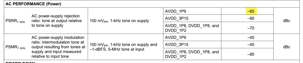
  1. AC PERFORMANCE (Power) - AVDD_1P9 PSSR: I noticed in the AC PERFORMANCE (Power) section that the PSSR of AVDD_1P9 is -65, which seems lower than other supplies. Can someone elaborate on how noise on this supply might impact the sampling output of the chip? Additionally, any recommendations on PDN impedance or accepted ripple current for this supply would be greatly appreciated.

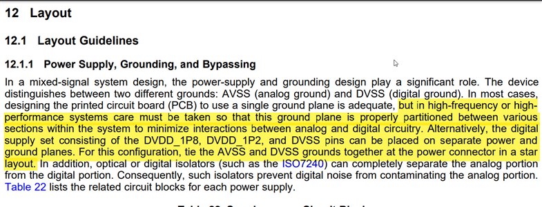
  2. Digital Ground (DVSS) and Analog Ground (AVSS) Connection: I'm seeking clarification on whether DVSS and AVSS are internally connected. To control the return current of the analog inputs, understanding how to split the grounds is crucial. Considering that SPI is shared between two dies, if a buffer IC is needed for SPI signals, should it be DVSS-referred or AVSS-referred?

  3. Board Layout - INPx and INMx Pins: In the "12.1.2 Board Layout" section, the recommended layout suggests isolating the INPx and INMx pin area by avoiding power planes under the INM and INP pins, and cutting the ground plane under these pins. I'm concerned about potential impedance mismatch and crosstalk. Can someone provide insights or suggest best practices to address these concerns?

  4. AFE5816EVM Design or Fabrication Files: I'm planning to purchase the AFE5816EVM, but due to our design schedule, I'm wondering if there's a chance to access the design or fabrication files of the AFE5816EVM or any layout examples from the datasheet.

I appreciate any insights or guidance from the experienced members of the community. Thank you!

  • Hi,

    1. Any noise on AVDD_1P9 samples will see rejection of -65dB at 1kHz. So we need to make sure that noise coming from power supply is lower than AFE output referred noise. At max gain, AFE output referred noise is ~200nV/rt(Hz). So noise at power supply should be at least < 200nV*10^(65/20) = 355uV/rt(Hz). In your system there will be multiple channels. Let say there are 128 channels and power supply noise will be correlated. Which will further reduce the noise spec requirement by sqrt(128) and also it will be better to keep supply noise half of device output noise. So allowed noise on power supply will be 100nV * 10^(65/20)/sqrt(128) = 15 uV/rt(Hz).

    2. This requirement is for the case when you are using demodulator in the device. Since AFE5816 doesnt support demod, you can have only single ground plane. No need to separate AVSS and DVSS.

    3. This requirement is for the case when you are using demodulator in the device. Since AFE5816 doesnt support demod, you can have only single ground plane and no need to separate INPx and INMx to quite ground plane.

    4. Design files are made available through MSS. Please reach out to mail id support_us_afe_tx@list.ti.com for further support.

    Thanks!

    Regards,

    Shabbir

  • Greetings and Happy New Year!

    1.
     Thank you for the insightful calculations. We'll ensure the power supply noise stays below 15 uV/rt(Hz) to meet the AFE5816 requirements.

    2&3.
    Appreciate the clarification. Our layout decisions consider the recommendations in "12.1.1 Power Supply, Grounding, and Bypassing" of the datasheet, emphasizing proper ground plane partitioning in high-performance systems.

    4.
    Thank you for the information. I'll be in contact through the provided email for further support.

    Best regards, 

    Peter