Hi team,
I understand ADD[2,1,0] decide which input CH is.
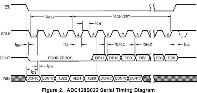
In timing chart, it seems that DOUT start before all ADD are decided. If ADD[] level is decided at timing of SCLK rising.
Actually, when ADD[] level is decided?
Best regards.
Goto
This thread has been locked.
If you have a related question, please click the "Ask a related question" button in the top right corner. The newly created question will be automatically linked to this question.
Hi team,
I understand ADD[2,1,0] decide which input CH is.
In timing chart, it seems that DOUT start before all ADD are decided. If ADD[] level is decided at timing of SCLK rising.
Actually, when ADD[] level is decided?
Best regards.
Goto
Hi Goto-san,
Thanks for reaching out. ADD[2,1,0] will actually be changing the input channel for the next conversion cycle. Here's some information from section 7.3.1 (Serial Interface) of the datasheet. "While a conversion is in progress, the address of the next input for conversion is clocked into a control register through the DIN pin on the first 8 rising edges of SCLK after the fall of CS."
Of note, the first conversion after power up will take data from IN0. Hope this helps, and please reach back out if you have any more questions!
Best,
Joel
Hi Joel-san,
Thank you for your support.
I understood that the rising edge of the fifth SCLK decides add[0] and decides the input address.
At this time, DB11 output start before the rising edge of the fifth SCLK. (Red line in the figure above)
Does output start before the input address is decided?
Many thanks,
Goto
Hi Goto-san,
The first bit containing data of the current conversion (D11) will not have been sent out by the time ADD0 is read into the control register because DIN is clocked on rising edges and DOUT on falling edges, but even yet it remains that DOUT is data for the current conversion, and the 8 bits of DIN, from which we only care about ADD2, ADD1, and ADD0, are being stored into the ADC128S022's control register for the following conversion cycle, and not the current one.
For example, before the very first conversion cycle after power up, which takes 16 SCLK cycles, the control register is set to all 0s, and so the first conversion will read from IN0. If you are not reading from IN0, you can discard this reading, but it should be valid if you do wish to use IN0 as one of your inputs. If during the first conversion cycle, you set ADD[2,1,0] to 001, you will only see this changed until the next conversion cycle, that is to say changing DIN will come into effect after the current conversion's DOUT is finished.
So in short, at SCLK's 5th rising edge, DOUT for the current conversion cycle (N) is holding to be read on the falling edge of SCLK, and ADD0 in DIN is being read into the control register to modify the input channel for the next conversion cycle (N+1). Please let me know if this helped clear this up more.
Best,
Joel