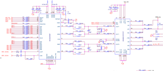
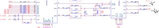
This thread has been locked.
If you have a related question, please click the "Ask a related question" button in the top right corner. The newly created question will be automatically linked to this question.
Hi Paulino,
How are you measuring the digital outputs? With a high-impedance probe? Also, the picture you sent is low resolution so I cannot see it.
Regards,
Geoff
Hello Geoff,
Thanks for getting back to me. I am using a logic analizer to look at the digital outputs for ch 2 (DB[7:0] and DCLK). I originally had default configuration through pins with 2's complement with external reference (REFBUF = 1.2V). N
ow, I am wondering if once I programmed binary format through SPI it requires all device configuration to be done through SPI. If so, can you share configuration values for all registers involved to configure binary format for both channels using external REFBUF = 1.2V?
I used the sample sch on figure 9-1 in DS for reference.
Br,
Paulino
Hi Paulino,
The entire SPI configuration should not need to be redone.
For the output data format, you just need to set bit 1 (data should be 0x02) for registers 0x8F and 0x92.
Regards,
Drew
Hello Drew,
Thanks for confirming device configuration is not needed after a SPI access, great. Now, for enabling offset binary it is also recommended to enable digital bypass through bit D2 in address 0x24. I will go ahead and enable this feature as well. Thanks for the feedback.
Paulino