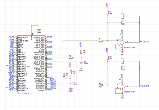
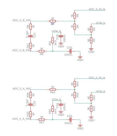
I'd like to use the AFE7222 in a design I'm working on. The IO will be a single pin for each ADC/DAC. How can I use the ADCs/DACs in single ended operation? Ideally, I would like to avoid using a balun. Thanks.

-
Ask a related question
What is a related question?A related question is a question created from another question. When the related question is created, it will be automatically linked to the original question.