- Ask a related questionWhat is a related question?A related question is a question created from another question. When the related question is created, it will be automatically linked to the original question.
Hi team,
Could you please help give some comments about the following questions? Thank you!
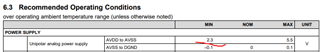
My customer is using the ADS1120-Q1 in the project, the power supply is CR2032b, voltage 2v~3V.
The bridge parameters are:
Piezo resistance:Min28kΩ,Typ33kΩ,Max38kΩ
The Y/Z axis has a maximum range of 400G
Y-axis sensitivity:0.10mV/g/V
Z-axis sensitivity:0.04mV/g/V
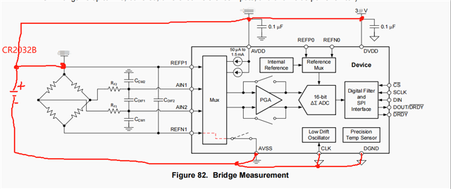
Q1:If ADS1120-Q1 can be wired as shown in the diagram below (REFP1, AVDD, DVDD to battery positive, AVSS, DGND, CLK to battery negative)?
Q2: Are the following calculations correct? Will the output of the detection bridge (±48mV) be satisfied when Gain=32, AVDD=3V?
Bridge output Vz=48 mV at 3V, 400G.
VIN (MAX) ≤ ±[(AVDD – AVSS) – 0.4 V] / Gain = ±(3V – 0.4 V) / 32= ±81mV
1 LSB = (2 * Vref / Gain) / 2 16 = (2 * 3 V / 32) / 2^16 = 2.86 µV
Q3: Is the 1LSB the minimum differential voltage that the ADS1120-Q1 can detect?
Regards,
Ivy