This thread has been locked.

If you have a related question, please click the "Ask a related question" button in the top right corner. The newly created question will be automatically linked to this question.

AVSS current increases as temperature rises

Part Number:  DAC7716
Other Parts Discussed in Thread: DCP020515D, , REF5050, ADS8883, OPA4990, DAC8234, DAC8734, PGA855

Tool/software:

Hello,

I am using two DAC7716 on our board and they are being powered by a DCP020515D part.  Through testing at around 75C we found that the DCP020515D would go into what looks like thermal shutdown because the output rails of the part are rock solid +/-15V until all of a sudden at around 75C they have huge amount of ripple at around 150KHz approx and I take that to mean that the part is going in/out of thermal shutdown?.

I removed the DCP020515D and used an external power supply instead.   As the temperature rose, I saw the negative supply current rise from 50mA to about 200mA by the time 85C was reached.  This indicated to me that the issue is not with the DCP020515D shutting down but instead there is a load problem.

Setting the board on the bench and continuing to use the external power supply, and now this time rather than heating up the entire board  I used a reflow pen at its lowest setting (100C) and kept the pen around 0.5-1 inch away from parts and move it around the board looking to see which semiconductors would cause an increase in negative supply current.   Moving the pen over the DAC7716 would increase the current by 50mA at the elevated temperature

Normal negative supply current is around 40-50mA at room temperature.  At around -30C the negative supply current is around 30-40mA..

Any suggestions?

  • Writing a 0x1BBC to the control register did not change the rise in current as a function of temperature..

    The issue seems to be more to do with the entire part rather than by channel.

  • Hi Mike, 

    What loads are connected to the DAC outputs when you are running this test? The supply current shouldn't be be 40mA unloaded. The short circuit limit of this part is actually 10mA, so this x the 4 output channels could be resulting in the ~40mA output you're seeing. 

    Best,

    Katlynne 

  • That was my understanding as well in terms of current consumption.  But all the outputs are either unloaded or drive very high output impedance lines.

    The outputs of one of the DAC7716 are unloaded.  The second one drives two loads that are >20K ohms and the remaining two go to a TMUX7309FRRPR which is currently disabled and the TMUX7309FRRPR supply pins are the same voltages that are delivered to both DAC7716 parts.

    What is odd is that even if I write a 0x1BBC to the control register to essentially turn off all the outputs (which I measure to be the case), I still see excessive current at higher temperatures.

    Please let me know next steps or things to test out.  Thank you!

  • Also, connected up the DAC7716EVM board fresh out of the box, just +15V, -15V, and 5V to the board with I/O jumper moved to +5V and exposed the DAC to 100C and the AVSS current did not move!   In this case there is no digital signals to the demo board. 

    The demo board contains a DAC7716SPFB whereas on our board we are using a DAC7716SRHAR.

  • On the boards we are having issue we changed the FPGA digital outputs to keep them all in a high state more closely emulating the demo board.  Exposed one of the DAC7716 to 100C and the current on AVSS rises significantly.

    Even tried manually bringing up the digital supply first followed by negative AVSS supply followed by AVDD supply.  Exposed one of the DAC7716 to 100C and the currents still rises on the AVSS.

    What are we missing?

    The only other thing that is different between our board with issue and demo board is that IOVDD gets 3.3V through TPS73733DRVR regulator and could there be a voltage sequencing kind of issue?

  • Another question:  What kind of things, regardless if they make sense or not at the moment, could cause excessive current to show up on the AVSS negative supply at high temperatures?  If I can get a list of those things, we can chase those and provide feedback.

  • Hi Mike, 

    I'm less concerned with the current rising when you increase the temperature, and more concerned with the fact that the supply current is 40mA when basically unloaded even at room temperature. I would expect that the part is damaged, or there is something on the device shorting to ground. Possibly due to how the part is soldered to the board. 

    Are both of the DAC7716 parts on your board experiencing this high current draw? Were you ever able to configure the DAC outputs for some output voltage, or has this issue been there since the first power on of this board? Are you able to read back from any of the registers? If the device is damaged or there is something wrong with the parts connection to the board then you wont get any data back. 

    Best,

    Katlynne Jones

  • As far as supply sequencing, we do share the requirements in the datasheet:

  • I should clarify that the total board current on the -15V is approximately 30-40mA.  If I heat up either DAC7716 the current will rise by about 50mA; the longer I have 100C on the part the closer it hits 100mA total for the board assembly (I focus the heat on the DAC7716.

    From about 65C (approx) down to -50C the DAC7716 channels work as expected and the -15V current is around the 30-40mA mark for the board assembly; above 65C (approx) the -15V supply starts to ramp up above the normal 30-40mA and at 85C is between 100-200mA (using external supply); normal supply shuts down well before those kinds of numbers.

    We are experiencing this issue across many board assemblies, more than 30 out of 200 that show the greatest severity, but likely it is across all the boards if I had to make an educated guess.

    We can work to readback all register values to confirm settings; but even if they are all jumbled up could that even remotely cause excessive AVSS current?

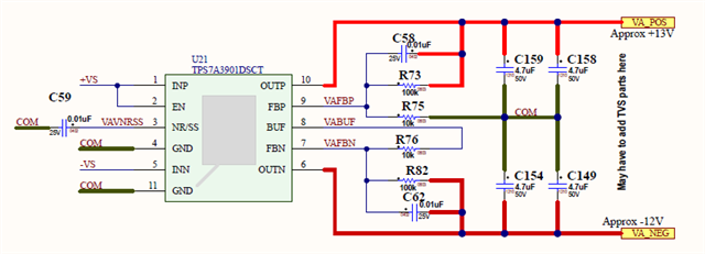
  • Oh, VREFs originate from the same +15V but goes through a separate TPS7A3901DSCT regulator.

    +5V -> DCP020515D -> +15V -> TPS7A3901DSCT -> 5.5V -> REF5050 -> DAC7716.REFs (orange trace)

                                                       ->  TPS7A3901DSCT -> 13V -> DAC7716.AVDD (blue trace)

                                             -15V  ->  TPS7A3901DSCT -> -12V -> DAC7716.AVSS (red trace

    If the 5.5V comes up before the 13V then that might turn on the ESD and could that be significant current draw like we are seeing?

    Here is the supply start up we are seeing on a typical board:  Green=+3.3V, Blue=+13V, Red=-12V, Orange=VREF

    One board has this start up which is odd and is the one that is drawing the most -15V current.

    Blue=+13V, Red=-12V, Orange=VREF

  • All the digital lines appear to be low until after FPGA programming.  In green is the chip select at the DAC7716.  Orange is VREF and the other two are +13V and -12V.

  • Hi Katlynne, wondering if you have any additional suggestions we can chase down?  I need to get this resolved ASAP. 

    If there is more information you need please let me know and we will get that information to you.  

    Thank you for your help,

    Mike

  • All of the parts we are having issue with come from the same lot of parts:

    TI Lot number:  3177938T43

    Wafer lot:  3003408UT1

  • Hi Mike,

    You can try powering the EVM with your boards supplies to see if the issue is replicated on the EVM part. 

    My thought is that something is causing the ESD cells to conduct and you varying the temperature is influencing the current flowing through the ESD diode. Trying to replicate the power sequencing on the EVM would help determine if the issue is really due to the sequencing, or some other damage to the device. 

    Best,

    Katlynne Jones

  • Is there a maximum current I ought to limit this test too?  

    What would cause the ESD cells to conduct?   Knowing that I can get laser focused on troubleshooting this.

    1. If AVSS and AVDD are at -5, +5 and VREF at 0.1 volt will that cause ESD cells to conduct (see scope image above)?

    2. If AVSS and AVDD come up at the same time will that work and what is the tolerance if they don't?  Is there a condition that would cause the ESD cells to conduct?

    3. Is it possible to latch the ESD cells such that once they are on, they don't turn off?   How can one make that happen?

    Where I am going with all these questions is I need to know how to recognize/identify when a combination of signals will induce ESD cell turn-on and/or latch-up.  Otherwise, I have no clue whether the relationships between signals is acceptable, etc.  

  • We powered the EVM with our board power supplies and it worked!

    We have ordered additional DAC7716 for overnight and will replace the parts on an existing board.   This will confirm whether it is DAC7716 parts or design.  Will provide update in 2 days.

  • Hi Mike, 

    Can you share your PCB layout related to this part as well? I reviewed the schematic again and it still looks ok to me. 

    Were you ever able to read back one of the registers on one of your boards to see if there is any successful communication happening with the device?

    I look forward to your update with replacing the parts.

    Best,

    Katlynne Jones

  • I can share the PCB layout but must be off-line.

    Replaced one of the DAC7716 and that seemed to work; local heating of the replaced part does not impact the power supply.  Replaced the second DAC7716 and now the problem has returned.

    In terms of communication, whatever we write out to the device appears to work as the values at the DAC outputs look quite good and correct for the given DAC values written.   To get read-back up and going will take about two days so I need to understand what information will be gained by doing so; is there something specific you are looking for?

    Under what conditions will the ESD cells conduct?   I appreciate the data on the power up sequencing but it is not clear in terms of tolerance.  When it says AVSS before AVDD or simultaneous, if it is roughly simultaneous how do we determine that it will not turn on the ESD?  My guess is that we have a very subtle condition?   When I power the board with an external +/-15V supply and manually bring up the -15V prior to the +15V that does not seem to have any impact.  The VREF will come up lagging AVDD as seen below. 

    AVDD(Orange) AVSS(Blue)

    AVDD(Yellow)_AVSS(Blue)

    AVDD(Orange)_AVSS(Blue,Inverted).   AVSS overlayed onto AVDD.  AVSS slightly lags AVDD, is this acceptable?

    AVDD (Orange), AVSS(Blue).  When AVDD is 1V (measured at cursor), AVSS is at -477mV.   Is this a problem?

    AVDD(Orange)_AVSS(Blue)_VREF(RED).   Is the VREF ramp acceptable?

    Mike

  • All of the digital inputs are driven by a weak pull-down at the FPGA ( /CS, SCLK, SDI, /RST, /LDAC, UNI/BIP-A, UNI/BIP-B ), until the FPGA is programmed.  Approx 100mS after AVSS and AVDD are up, the digital lines will revert to normal operation.  Is this acceptable?

  • Also, DVDD (5V) will lead IOVDD (3.3V) because the 5V drives the 3.3V LDO (TPS73733).   

  • Here is layout at one of the part locations.  This might be enough to evaluate thermal?

    This is the top layer in red.  There are 16 vias in the center pad that punch down into the ground plan on layer 2 and another ground plane on layer 5 and also into layers 2 (bright blue) and 3 (brown).

    Ground plane layer 2 in green, where there is green there is no copper.

    Ground plane layer 5 in dark red, where there is dark red there is no copper.  this extends to the right by 1/3 inch, to the left by 1.25 in, up about 3/4 inch, and down about 1inch.  Same is true for layer 2 and 3. 

  • I just noticed this in the datasheet on page 2.

    "(2) AVSS must be < –3.5V if AVDD ≥ 1V."       This is clearly not the case per waveforms.  The next question is how to change this?

    This is the supply.  DAC7716.AVDD = VA_POS.  DAC7716.AVSS = VA_NEG.

  • Hi Mark, 

    You do not need to do the readback test if you have confirmed that the DAC outputs are responding to communication. To be clear, is this the case with both the good and bad DAC7716 devices, or just the good? Is it possible to completely remove any output loads from the DAC and repeat your heating tests?

    When you say: 

    Replaced one of the DAC7716 and that seemed to work; local heating of the replaced part does not impact the power supply.  Replaced the second DAC7716 and now the problem has returned.

    Is this all on one board? Is is possible to do an A-B-A swap with the confirmed good DAC7716 and bad DAC7716 to check if the issue follows the part of follows the position of the part on the board?

    The most important factors of the supply sequencing are that the digital supplies power on first, and vref is powered on last. It's fine that DVDD will lead IOVDD as long as they are the fist supplies up. This looks to be the case based on your latest waveforms. The digital lines being pulled down by the FPGA until the analog signals are powered on is fine.

    I've been able to find that the reason for the recommendation of AVSS must be < –3.5V if AVDD ≥ 1V is that there is a diode internal to the device that would cause AVDD to draw higher current and heat the DAC when AVSS is not powered. As long as this is for a short time (on the order of ms), this shouldn't be a problem and would resolve itself when the AVSS < –3.5V if AVDD ≥ 1V condition is met. 

    Best,

    Katlynne Jones

  • Katlynne,

    The devices always work.  I can run a series of test software which sets the DACs and is readback by the ADC.  Even manual operation they all look very good, regardless of good/bad.  It is only when the board gets up to around 75C that the DCP020515D goes into thermal limit as the +/-15V look bad and then as temperature drops they snap back and look great.  If I heat either DAC7716 I can see the -15V begin to drop which tells me that the AVSS current of the DAC7716 is increasing.  If we remove the DCP020515D and power with external supply, we definitely see the AVSS (-15V) current increase as we heat up either DAC7716.  

    We have two DAC7716 on one board assembly.   We will perform more testing of swapping parts as you suggest.  I suspect that the problem follows the location not the part, but have not verified.  I want to remove both parts, and then add one back at a time, is the next step.

    We will do one more set of power up test waveforms to include DVDD and IOVDD, highly certain the sequence is happening, but just to be sure. 

    Any additional things we ought to try?

    Thanks,

    Mike

  • Additional tests performed:

    1. Removed voltage reference (REF5050) and that did not make any difference.  Ran up to 75C and same issue.

    No_REF5050_but_VREF_jumps_to_2V5

    What is weird is that after FPGA talks to DACs the VREF jumps from 0V to 2.5V.  The only things connected to this is the ADS8883.VREF pin 1 input and OPA4990 two + inputs.  Shorting to ground and power cycling and running up to 75C still have the same behavior current issue. .

    3. 3.3V(Blue)_+13V(Orange)_-12V(red)

    The data keeps pointing to the parts but cannot prove that anything external is a cause and effect.  The only externals are power (AVDD, AVSS, IOVDD, DVD) and VREF, and FPGA data lines to the DACs.     I am stumped and under big pressure as it is holding up shipments up the supply chain.  Need help to understand.   Seems like it is down to power supply?

    The demo board seems to be immune to this issue and the only thing we have not done is tie the +3.3V to the IOVDD, normally we have been connecting it to +5V.

    Trying to think of other stones to turn over without making any assumptions:

    What power supply event could cause AVSS to have larger currents than usual at high temperatures?

    Could there be a power down sequence that is damaging (this is something we have not explored)?

    VREF is using a REF5050 with about 24uF of capacitance (note: there is a 20K resistor in parallel with the 24uF cap).  The 24uF is 4.7uF x 5 caps.  Maximum energy is 300uJ or RC=0.5sec.  If there is rapid power cycle prior to decay, this would mean that VREF>0 and is active prior to AVSS and AVDD.  Could this cause damage?

  • Hi Mike, 

    If you remove the REF5050 on a good DAC7716, do you still see the spike to 2.5V on the reference pin? 

    Typically we recommend to power off the device in the reverse sequence that it is powered on. In this case, the sequencing is just related to device initialization. If the analog supplies are powered on first then the part has the potential for undefined behavior during operation as the digital did not run through it's initialization, but this is resolved on power cycle. What is your power down sequence? 

    Have you measured the DAC outputs & supply lines on a scope during your heating test to check for any abnormal behavior there?

    Your schematic shows the VMON pin as open, but your layout shows the pin being routed to something off page. Are you using VMON?

    Best,

    Katlynne Jones

  • I will have to scope capture the power down.  Will follow up on that.

    Yes, watched the supply lines during thermal tests, when we get to about 75C the AVSS currents from the DAC7716 get large enough that it causes the DCP020515 to go into thermal limit as the negative supply drops to around 8V average with lots of ripply and the positive supply is probably around 8-10VDC.  I can provide those waveforms as well.  The higher the temp the worse it gets.

    For one of the DAC7716 the VMON is open, on the second DAC7716 it is routed to a multiplexer input.

  • Hi Mike, 

    Yes, watched the supply lines during thermal tests

    What about the DAC outputs? And are you enabling VMON to connect to any of the DAC outputs during your initialization? 

    We will perform more testing of swapping parts as you suggest.  I suspect that the problem follows the location not the part, but have not verified.  I want to remove both parts, and then add one back at a time, is the next step.

    Any update with the test to swap the two parts?

    Best,

    Katlynne Jones

  •  

    Yes, watched the supply lines during thermal tests

    What about the DAC outputs? And are you enabling VMON to connect to any of the DAC outputs during your initialization? 

    No.

    Any update with the test to swap the two parts?

    This is my next step.


  •  

    Yes, watched the supply lines during thermal tests

    What about the DAC outputs? And are you enabling VMON to connect to any of the DAC outputs during your initialization? 

    No.

    Any update with the test to swap the two parts?

    This is my next step.


    When thermal limit at around 75C is reached the +15 and -15V looks like below, not surprising since currents on AVSS are large.

    13V(red)_-12V(Orange)_thermal_limit_DCP020515

    Startup_+15(Orange)_-15(Red)_IOVDD(Blue)_5VREF(green)

    Power Down sequence_+15V(Red)_-15V(Orange)_5VREF(blue)_3.3VIOVDD(green)

    PowerDown_one_of_two_DAC7716_Removed.  The run down time on VREF is longer.

    OnlyOneDAC7716_85C_-15V_has_severely_eroded to due_excess current.  Channel 3 (-15V is at about -9.5V)

    BothDacsRemoved_Notice_+15V_-15V_are_very_good  (both at +/-16V resulting from minimal loading).  The loads are clearly from the DAC7716 parts!

    Add to the power supply the DAC7716EVM with following connections:

    J3.1 to +13V of board

    J3.2 to -12V of board

    J3.6 to GND of board

    J3.8 to +3.3V of board

    J3.10 to +5 of board

    J1A.20 to 5V VREF of board

    Set temperature 90C.  You can see that the +/-15V are only slightly loaded.   The only difference with this setup is that the digital lines are not tied from the FPGA to the DAC7716EVM (it was determined that it was not important LDAC='0', UNI/BIP_A='0', UNI/BIP_B='0', RST='0', all others pulled up), and the 5V reference is tied through RC networks on the DAC7716EVM.  All DAC outputs are unloaded.  Further the system was power cycled while at 90C several times (3 times) and same results.  This proves that the power supplies are not negatively impacting the parts, this leaves VREF.

    Removed the DAC7716EVM and installed a new DAC7716 onto the board, thoroughly cleaned and dried.  Set temperature to 90C.  This DACs VREF inputs is driven by the other DAC, and so in this case this dac has floating VREF inputs.  All outputs of this DAC7716 are unloaded..  Observed results show significant loading of the -15V supply as it is average value has dropped from -15V to -8V.  At power up the FPGA will communicate sending gain and offset values only.

    My conclusion is that the QFN parts behave differently than the QFP parts.  QFN parts do not conform to the AISS specification as defined in the datasheet.  We have consumed 500 parts across boards and trying to figure out next steps.

    Are the DAC8234 and DAC8734 from the same process or are those constructed differently?  Is there a possibility that these parts behave differently in the AVSS current?

    I am going to do one more test by soldering a QFN to a schmart board and independently powering the board with a linear power supply as an independent verification.

  • Hi Mark, 

    The two device packages should not be behaving differently, but let's let your independent test reveal that. Right now the only thing I take away from this is that there is something different between your layout/ output connections and the EVM's, not that the issue it is package related. I'm also not confident that it is sequencing related, but again, let's let your independent test reveal that.

    When you try this test on the schmart board, please replicate all of the conditions that you are using on the EVM. This would be connecting the supplies as you've been doing, pulling up all digital to IOVDD, leaving outputs unloaded. 

    If the above test results in no issues, connect all of the digital of your board (with the FPGA source) to the digital pins of the device on the schmart board. Power up both your board and the device on the schmart board at the same time so you can replicate the digital startup behavior. 

    If this test results in no issues, connect the output loads of your board to the outputs (excluding the vmon pin) of the device on the schmart board. Again, power up both your board and the device on the schmart board at the same time so you can replicate the analog loading behavior. 

    Finally, if no issues up to this point connect the vmon pin. 

    Ideally the above would be done with no DAC7716 devices populated on your boards. If there is no issue when doing these above tests then that would rule out any sequencing/startup/loading concerns. 

    Both of the devices you mentioned are from the same process and have much of the same internal design, so I would expect they behave the same. The only major difference is the resolution. 

    Best,

    Katlynne Jones

  • OK, fair enough.  I will use your guide.  I have used TI parts for 35 years and rarely have there been any technical issues. Rarely it is the part, but it is the only thing I can attribute.  Hopefully this next test will reveal the smoking gun.

    The VMON is not connected on one DAC and the other DAC VMON is wired into a TMUX7309FRRPR pin 5.

  • I just noticed that for the thermal pad the datasheet indicates pad to be left floating or tied to AVSS.  We have it tied to our system common (same as DGND and AGND).  Could this be the issue?

  • Hi Mike, 

    I'm waiting for confirmation on this but it does look like the thermal pad is electrically connected to AVSS. I'm also trying to get a more detailed explanation from the design team as to why shorting ground to AVSS would cause this behavior. Hopefully they'll get back to me by Monday. 

    Were you able to do the schmart board test while leaving the thermal pad floating?

    Best,

    Katlynne Jones

  • We will have the schmart board setup ready to go on Saturday, finally.  It is not quite ready yet.

    Thanks,

    Mike

  • Schmart board:  Had all digital inputs pulled to IOVDD just like demo board, but with RESET tied to ground (same setup as with DAC7716EVM in prior test).  Did not tie the center pad to anything.  Wired up schmart board to existing board using same +13V (AVDD), -12V (AVSS), +3.3V (IOVDD) and +5V (DVDD) and COM.   Ran up to 90C and unregulated DCP02 voltage remained at +/-16V approximately!  No excessive currents!

    Have another board with both DAC7716 removed and on one DAC cleaned center pad (both on part and PCB) and placed a 2mil polymide tape and solder the part onto the board and placed the cleaned up DAC7716 on top of that.  Soldered to the board; was challenging as 2mil is way too high.  Anyway, got same high current results at high temperature.

    Repeated the above with a fresh DAC7716 and it works!!!   The unregulated +/-15V remain at +/-16V.  No significant loading.  The initial communication from FPGA provide the correct outputs at the DAC.

    With center pad tied to ground that must result in some kind of damage?   I need to know what is the potential impact/risk for the parts with center pad tied to ground rather than float or AVSS as we need to communicate with existing customers as we have 234 boards out in the field currently.

  • Hi Mike, 

    Thanks for sharing your results. 

    Yes, it is likely that the excess current (especially at the magnitudes you were seeing at hot temps) caused permanent damage the device which is why the issue persisted even when you isolated the thermal pad connection.

    I'm still trying to check with the design team to see if they have an idea as to why the outputs would still be functional despite the short (the excess current @ high temps being the only side effect). Were you setting the outputs to a positive or negative output? If you were setting them to a positive output voltage then the damage is likely in a non critical path for the outputs you were setting. I was also checking to see if they had any ideas as to why the current would be changing at higher temperatures. The original designer is not on the team anymore, but I was hoping to at least get a general explanation. I just asked for an update. 

    Best,

    Katlynne Jones

  • Hi Katlynne,

    One of the DAC7716 its outputs are set to 2.50V, 5.0V, 8.9V, -9V.  All of these outputs remain fixed and drive high impedance loads.  The second DAC7716 we have run many tests from -10V to +10V on all four channels.  These outputs are looped back to our multiplexed analog input channels that are all high impedance. 

    Any additional insight is much appreciated.  This has been deployed in an aerospace application so we need to be as clear as possible about any risks.

    If we tested either of the part locations, they worked perfectly from -50C up to about 65C approximately and then from 65C to 85C is when AVSS currents tended to rise up linearly roughly ( to about 50mA to 75mA).  As the AVSS current rises the DCP020515D negative output begins to reduce from -15V and by the time we hit DAC7716_AVSS current of 50mA to 75mA, the DCP02 negative voltage is already around -11V or less and heading into thermal limit.   When temps fall back below the 70C approximately then everything returns to normal; ran a lot of tests and this repeats all the time and DAC outputs all look good at that point.   

    It might be that the DCP020515D along with post linear regulator TPS7A3901 limit the maximum power that can be delivered to the DAC7716; the maximum current observed at the high temperature is around 50mA to perhaps 75mA on AVSS and AVDD hardly changes and well within expected values. 

    Max power at AVSS is on the order of ( 75mA + 4mA * 4 ) * (-12V) = 1.1W (outputs driving high-impedance loads).   Max junction temperature 150C, ambient at 90C and thermal junction to ambient 32C/W =>   1.1W * 32C/W + 90C =  125C.    Perhaps, it survives, sort of, due to the upper current limit imposed by the power supply.   Even parts that I have had on the board driving with external power supply with currents into the 200mA range seem to have survived, but I don't know its long term reliability as the power delivered to the DAC7716 could have been into the ( 80mA + 4mA * 4 ) * (-15V) = 1.44W => 1.44W * 32C/W + 85C = 131C.  The thermal resistance is probably less than 32C/W and above 20C/W.

    Thanks,

    Mike

  • Hi Mike, 

    Not all damage results in loss of total device function. Though it may seem like some parts "survive", to what extent would be unknown. I'd agree with you that the temperature limit would prevent the device from completely blowing up. 

    Perhaps, it survives, sort of, due to the upper current limit imposed by the power supply.

    As far as risk, I would not recommend using this design as is. We'd have no way to predict part to part behavior, or long term behavior of the parts being operated under this condition.

    Based on the feedback from the design team, where the damaging current actually ends up in the device depends on the DAC state and transient conditions, and is essentially unpredictable. There are many areas in the design (hence the unpredictability) where the current induced by the thermal pad grounding could travel and create a forward biased p-n junction, damaging that portion of the device. As far as the temperature response, this makes sense. The p-n junction would have a negative temperature coefficient which explains the increase in current as you were increasing the temperature. 

    Best.

    Katlynne Jones

  • We are trying to determine next steps and have some follow up questions:

    If we collect up a few DAC7716 can we send them to you for further analysis to determine the resulting defect?   

    One of the DAC7716 is communicated once at power up and remains static; the communication is always the same.  That part has a defect as you described, but the outputs are always correct except at high temperatures.

    I suspect that since we have two DAC7716 powered by a 2Watt source that the maximum power that is dissipated by either of the DACs is at most 1.3 Watts.   32C/W * 1.3W + 85C = 127C which is always below maximum junction temperature.   Out of 500 parts we have not seen one catastrophically fail and we have had those running for several months.

    We have had a couple of boards we have been using for months, power cycling, thermal cycling and neither of the DACs have catastrophically failed, and they always produce the correct outputs.  They have a defect like you describe, but always work.  Trying to judge  the urgency of replacement.   Seems like, other than at high temps (which is limited by 2W DC-DC), the expected outputs are always correct and we have many boards that have been operating properly for months without issue and the longer it operates the less likely it will totally fail?

    Would this defect be similar to an ESD event?  If so, how might that play out?

  • Hi Mike,

    We are reviewing this and will back to you shortly.

    Thanks,
    Lucas

  • Any update?  I need to follow up with customers.  Thank you for your help.

  • Hi Mike,

    Per you findings "With center pad tied to ground that must result in some kind of damage?   I need to know what is the potential impact/risk for the parts with center pad tied to ground rather than float or AVSS as we need to communicate with existing customers as we have 234 boards out in the field currently."

    I think we have an explanation here.  On some devices (in general, not just DAC7716) the thermal pad is electrically connected to the die substrate or only connected using a thermal conductive material.  The issue, as I see it, is that even when the pad is electrically conductive to the substrate, it is generally a high-impedance connection.  What we are likely seeing is that at hot temperature that impedance is increasing and causing the ESD cells on VSS to be reverse biased to GND.  These can get damaged when sustaining current as it is a much greater charge than they are designed to handle.  

    I would bet that if you removed one of the appearly damaged devices you would measure a different impedance from the thermal pad to GND/VSS than on a new unit.

  • Hi Paul,

    For clarification:  

    What we are likely seeing is that at hot temperature that impedance is increasing and causing the ESD cells on VSS to be reverse biased to GND.

    Do you mean impedance is decreasing within increase temperature?

    Is it possible to send parts back for analysis?

    Thanks,

    Mike

  • My suspicion is that at some critical temperature, we will see a increasing leakage current, until it we have a high-current condition.  I would expect more of a diode behavior than a resistive behavior, but yes, you would see some impedance change.

    To clarify, the in this case you have the substrate biased to your vss supply, but at some critical temperature, the thermal pad (GND) will start conducting.

  • This design error is a pain to detect and on our end it cost us significant amount of time and costs.  There is no symptoms exhibited at room temperature an is only seen at elevated temperatures and severity will vary from part to part.  In our case, with the DCP020515D providing +/-15V to two of the DAC7716 this becomes mostly detectable at high temperatures.  Had we powered directly the DAC7716 to higher power capable +/-12V, for example, this issue could have gone undetected which would result in long term reliability problem (due to excessive power dissipation at the DAC7716 at high temperatures). 

    Further, the demo board only contains the QFP and not the QFN. There is no example schematic using a QFN in which to capture/remind proper connection of the center pad. 

    Due to risk you ought to update the datasheet by adding a PCB connection summary checklist section:

    • Thermal pad connection
      • Reason: if connected to ground it may be undetectable depending on AVDD & AVSS power supply power capability and it in some cases lead to reliability issues if DAC7716 supply currents are not limited.  Make reference to pinout description on page 7 for further details. Explicitly add the center pad to the pin description table!
    • Power supply sequencing
      • Reason: If done incorrectly means a PCB re-spin and a bunch of back-forth with TI to .   In this case adding a typical power supply waveform illustrating startup sequence is highly desirable as it brings further clarity.
    • Re-iterate or point out which notes within the datasheet to pay particular attention to with respect to power supplies (i.e. note 2 on page 2, note 4 on page 3, note 14 and 15 on page 5,

    The demo board schematic ought to have a note suggesting that if a QFN is used to affirm that the center pad of the part be either left floating or tied to AVSS.

    I have seen checklists for larger parts and that helps a lot because some datasheets can be 1000 pages long and it is incredibly easy to miss a detail.  Now, imagine you have 25 parts on a board each with 40 to 1000 page datasheets each (1000 to 5000 pages to read in detail); it is incredibly high risk that something will get missed; datasheet summaries are essential in today's world.   The summary lists are big risk reducers for customers and helps us get to market faster and ultimately buy more parts which is really then end goal.

    Also, the datasheet is not very clear about the gain adjustment and how the voltage error is calculated.  When the datasheet is updated it will be very valuable to give more clarity with respect to that issue because we currently have parts that provide a full +/-10V range but there appears to be an offset which when calibrating at zero we do not see....this is another topic, but adding for completeness.

  • Hi Mike, 

    I appreciate your detailed feedback for the datasheet/EVM user's guide. I'll mark your points down for future updates.  

    Best,

    Katlynne Jones

  • We also designed in a PGA855 which has the center pad tied to -VSS correctly and I suspect it was because it was mentioned in the pin table list.  In other competitor product it is mentioned in the pin table list, note by the top view of the part both in verbage and a -V is added to the center pad (3 places).

    -

    We are looking at reworking boards to apply a soldermask over the center pad on the PCB to achieve electrical isolation, this appears to work.   Does the center pad need to be mechanically soldered to the board?  If it does, can an underfill or glue be an acceptable alternative?  This is a long term mechanical reliability question and determination of a the best rework solution.   Maybe this needs to be posted in a different part of the forum?

    Are there ways to calculate required mechanicals so that if we decide down a path we are guaranteed to meet the requirements similar to soldering the center pad to the PCB?    The datasheet has no detail around this.

    -

    In terms of thermal I don't see any issue in not soldering the center pad; tell me if the calculation is incorrect, but even if the thermal resistance was three times the 32C/W we would still be well below max junction temperature at 85C.  Worse case power calculation:

    DVDD*DIDD + AVDD*AIDD + AVSS*AISS + ILOADs * Vloads

    5V * 50uA + 15V * 3.4mA + 15V * 4.0mA + 4*3mA*10V = 0.23W.   

    Thermal resistance Junction to case = 32C/W

    Delta_temperature = 0.23W * 32C/W = 7C.     

  • Hi Mike, 

    I reached out to the packaging team for comment. Here is their response:

    "The RHA package is pretty large (6x6) so it is best to solder the exposed pad because it helps to absorb some of the work put into the solder joints from CTE mismatch over temperature cycles. Not soldering it would lead to an earlier failure of one of the critical leads, one most likely near a corner of the package.

    However using epoxy is a big risk for long term reliability. Epoxy has a different CTE than solder so the expansion rates will be different over temperature. I suspect the CTE of the epoxy is likely larger than solder and would basically expand at a higher rate in the center of the package and crack a joint pretty quick.

    For reliability it’s probably best to scrap the PCBs and fix the connection of the center land to what it needs to be. I would be really hesitant to use epoxy or any other adhesive in the center."

    Best,

    Katlynne Jones

  • Hi Katlynne,

    CTE = Coefficient of Thermal Expansion?

    What does it mean that the exposed pad helps to absorb the work put into the solder joints from CTE mismatch?

    What is the CTE of the part exactly?  Is there any non-conductive materials that could be used in place of solder at the center pad?  We are looking for ways to electrically isolate. 

    Mike