Other Parts Discussed in Thread: ADS7841
Tool/software:
Hi,
I am currently working with the ADS7481-Q1 EVM (BOOSTXL-ADS7841-Q1) and have encountered some difficulties in obtaining accurate ADC values.
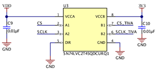
I have interfaced BOOSTXL-ADS7841-Q1 with the application FPGA having IO voltage level 3.3V and connected all the signal line (SPI lines, SHDN, etc.) on the connector J1 or J2. VDD & 3.3V power pins are at 3.3V as no level shifting needed.

Despite following the guidelines and specifications provided in the documents, the values we are receiving do not align with expected results.
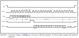
Expected signals with 24 clock conversion from datasheet:

Here are specific details about the issue we observed:
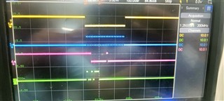
- BUSY Signal is not getting High, when CS becomes high after 24th Clock Cycle.
- According to graph given in Datasheet, Busy should be high just after Data is send to ADC (after 8th clock), but in the Image below BUSY line is not getting high after 8th clock as per Datasheet.
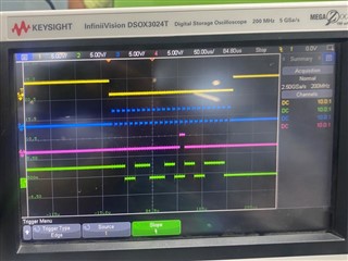
- We are not getting expected ADC value on SDO line, and it is fluctuating.
We observe below waveforms on signal lines when we connect ADS7481-Q1 EVM with CAN FDL FPGA -
1. Color code: Yellow -> Chip select(CS), Blue -> Clock, Violet -> BUSY signal, Green -> SDI (To ADC)

2. Color code: Yellow -> Chip select, Blue -> Clock, Violet -> BUSY signal, Green -> SDO (From ADC)

(Due to Limitation of DSO channels SDO Signal is shown in above image with respect to same CS, CLK, BUSY.)
What should be correct sequence of CS, SDI, SDO, SCK, BUSY signals?
Is there anything different we have to try in order to make ADC work?
Many Thanks!
BR,
Vaibhav

