This thread has been locked.

If you have a related question, please click the "Ask a related question" button in the top right corner. The newly created question will be automatically linked to this question.

ADS131A04: Non-linear Response

Part Number: ADS131A04
Other Parts Discussed in Thread: AMC1350, THP210, LM7705

Tool/software:

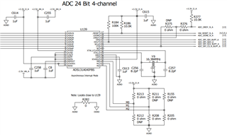
For this circuit, we have a signal that is +/-7.5VDC input and want to read it on the ADC. We send the input signal through the AMC1350DWVR (U39) to isolate the signal from our digital ground. Then we send it through a low pass filter with a gain of 1.25 using the THP210DGK (U44). This then goes through the AAF circuit R263, C356, R338, C324, and C331 to go into the ADS131A04 ADC (U139).


For the ADC we have the Fmod = 2.048Mhz and the OSR to 2048 to sample at 1000Hz.

The issue we are having is when it reaches the AAF filter our circuit is no longer linear.


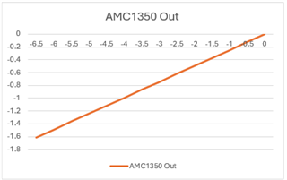
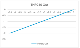
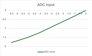
Below, is 4 points in the circuit I looked at for troubleshooting.

Input (Blue): Input of the analog chain that goes from -6.5VDC to 0VDC in -.5VDC increments.

AMC1350 OUT (Orange): Output of the AMC1350, U39

THP210 OUT (Light Blue): Output of the THP210 circuit, U44

ADC Input (Green): Input of the ADC
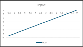


From these charts, I am noticing everything is linear up to the ADC input.  I have tried adjusting my cutoff frequency of the RC circuit before the ADC but no luck.


Below is the data measurements used for the graphs above. It shows the gains are similar to what the design goal was besides the ADC input circuit.


Input

AMC1350 Out

THP210 Out

ADC Input

-6.497

-1.6116

-2.0016

-1.7798

-6.004

-1.4887

-1.8491

-1.6847

-5.508

-1.3656

-1.6963

-1.5849

-5.0095

-1.2424

-1.5431

-1.4765

-4.5112

-1.1186

-1.3894

-1.354

-4.0141

-0.9952

-1.236

-1.2176

-3.5026

-0.868

-1.0782

-1.0696

-3.0159

-0.7471

-0.928

-0.9247

-2.5174

-0.6232

-0.7742

-0.7732

-2.019

-0.4994

-0.6202

-0.6199

-1.519

-0.375

-0.4659

-0.4656

-1.0182

-0.2506

-0.3114

-0.3113

-0.5166

-0.126

-0.1566

-0.1566

-0.0153

-0.0015

-0.0019

-0.002

  • AMC1350_Voltage_Monitor.TSC

    Here is the TINA model I used to test the circuit before I implemented it. I do not have the ADC in the circuit, but used the input capacitance and impedance and it shows to be linear through a DC analysis. 

  • Hi James,

    Welcome to the E2E forum.

    I did not see any circuit for those components you mentioned (R263, C356, R338, C324, and C331), did you upload or miss it? or they have the same values as shown in the simulation circuit in TINA?

    Did you check the output of AAF after disconnected the ADC from the AAF?

    Regards,

    Dale

  • Don't think my attachments worked. Here are the screen shots for those components. 

  • I did check it when I was disconnected from the ADC, it works like the simulation shows.

  • Hi James Frisbie,

    Dale is out of the office today returning on Monday. He will review your response then

    -Bryan

  • Hi James Frisbie,

    Thank you for your patience. I noticed that you are not using the negative charge pump because you directly shorted the VNCP pin to AVSS. Could you disconnect VNCP pin from AVSS and insert a 270-nF capacitor to AVSS then enable the negative charge pump by setting VNCPEN bit to 1 for test purpose? just repeat the test after you change them and let me know the result, thanks.

    - Dale

  • We are using a bipolar analog supply. On page 81, one of the "don't" is to use the charge pump with a bipolar analog supply if I am reading that correctly.

    I believe it has to do with the common mode voltage offset. I had the THP210DGK using a 2.5V common mode voltage. I was expecting since we have the 4V internal reference on the ADC enabled that I could swing my voltage +/-1.5VDC but doesn't seem like the case. Becuase we are using a bipolar supply, do I only have the range of +/-2.5V including the common mode voltage?

  • Hi James,

    Yes, this ADC can support dual power supplier. What I asked is just for test purpose.

    I just noticed 2.5V common-mode voltage this morning, your signal is shifted to 0~5V range using THP210 with the 2.5V common-mode voltage, so you actually do NOT need a +/-2.5V power supplies for ADS131A04 ADC. A single +5V power supply (AVDD=+5V, AVSS=GND=0V) can be used for your ADS131A04 while the internal charge pump is disabled.

    Best regards

    Dale

  • I believe it is the common mode voltage. We set the internal reference on the ADC 2.442V, this was causing the issue. I was adjusting the gain and common mode voltage of the THP210 so the ADC would see the entire analog chain signal. Also, I also tried changing the THP210 so that it had a +2.5V and -2.5V on V+ and V- with a VOCM input at 1.25V, this worked as well.  I noticed when I tied the THP210 VOCM to ground its common mode voltage was ~.8V but as the differential signal increased it rose to ~1V. I have a couple questions now:

    1. What is the common mode voltage for the THP210 when VOCM is tied to ground? 

    2. Is there a configuration I should use to have the best accuracy? 

  • Hi James,

    The VOCM of THP210 is an input for output common-mode voltage control, you should not tie it to the ground when THP210 is powered by a single 5V power supply, but you can tie it to the ground when the  THP210 is powered by a dual power supply (e.g. +/-2.5V). I'm not an expect and a right support engineer for THP210, you will have to post your questions about THP210 to the amplifier E2E forum.

    The output of the AMC1350 is a differential analog output, so one of the following options can be used to measure the signal from AMC1350:

    1. The THP210 is powered with a 5V supply for VS+, the ground for VS- or a –0.232V negative supply generated by the low-noise negative bias generator (LM7705) allowing additional headroom for output swing to GND with ultra-low distortion as shown in Figure 9-16 in THP210 datasheet, the VOCM is set to 2.25V. ADS131A04 is powered by a single 5V supply while the internal charge pump is disabled.
    2. The THP210 is powered by a dual power supply (e.g. +/-2.5V), the VOCM can be set to the ground. ADS131A04 is powered by a dual power supply (e.g. +/-2.5V) as well and the internal charge pump is disabled.
    3. You could also use a 3V power supply for ADS131A04 with or without a negative charge pump but you will have to attentude your input signal more with THP210.

    You existing schematic is mixing to use the 1st and 2nd option.

    BR,

    Dale

  • I think I found a 4th option that seemed to work. I kept the THP210 at +5 and GND as it does not cause a PCB spin. I then used a voltage divider on the +2.5V VOCM signal to create the offset at 1.25V. This allows me to create me gain stage to have a 1.1V/V gain and my signal should have a +/2.2V signal reference at 1.25VDC. For AIN+, it will be 2.35V max and should no longer clip nor exceed the differential +/-2.442 that we are using at the reference. Do you see anything wrong with this method, or do you think it's best to go to option 2? I've tested both in the lab and I am getting similar results, but I've only tested at ambient temperature so far. 

  • Hi James,

    For the 4th option, do you mean your signal to the ADC's input is sweeping at +1.25V DC (VCM) and the differential voltage is +/-2.2V? Is the ADC still powered with +/-2.5V power supply?

    BR,

    Dale

  • Yes, the peak voltage for AINxN/P is 2.45V and .05V that is within the rails still.

  • Hi James,

    Thank you for your clarification. Your option 4 works as long as a divider is used to create a 1.25V DC. When the absolute voltage on the AINxN/P is 2.45V and .05V, the differential voltage is +/-2.4V.

    BR,

    Dale