This thread has been locked.

If you have a related question, please click the "Ask a related question" button in the top right corner. The newly created question will be automatically linked to this question.

ADS7038: Erroneous ADC values being returned

Part Number: ADS7038

Tool/software:

I checked the TI forums but could not find a definitive solution so am posting a new question.

I have a problem with the ADS7038 chip. I seem to get wrong ADC values every now and again. This happens on my production card but I have also recreated it with just an NXP S32K146 development board talking to a TI ADS7038 development board. I believe it might be an SPI clocking issue.

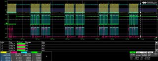
I have some oscilloscope JPGs and CSV readings that show interesting/weird effects. These come from my production card but I will aim to get some traces from the NXP/TI combination to eliminate our production card design from the equation. This will take a few days.

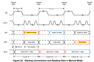
I am reading from ADC channel 3, with the channel number appended, so in the 24 bit MISO return from the ADC I should be getting 0xABCd00 where 0xABC is the ADC value and d is the channel number (3).

I inject a sawtooth input from 1V..2V at 1Hz and/or 1KHz. I have AVDD set to 3V. This should mean that I expect values in the range 1300..2730.
I send a WRITE, CHANNEL_SEL, 3 and then a WRITE, SYSTEM_STATUS, 0 and get the ADC reading on the 2nd command. I then repeat this sequence (currently as fast as possible, but it also fails when run at a fixed frequency - where the original problem was found).
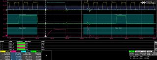
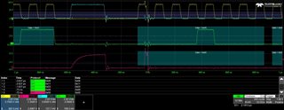
I have modified my code so that if I get a non-3 channel number or ADC reading < 100 or ADC reading > 3700 then I send an (invalid) SPI message 0xDDEEFF and halts at a breakpoint. I have the oscilloscope stop recording when it sees this 0xDDEEFF value.
Ideally the code should never hit the breakpoint and the oscilloscope should never stop recording. Unfortunately neither is the case as shown in the JPGs.

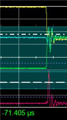
The JPGs, especially the final one, show ADC readings increasing (due to the sawtooth input) 0x7cc, 0x7e1, 0x7f1, 0x000, 0x80c (the 0x000 is the erroneous value).
Interestingly on the 0x000 there is an attempt by the ADC to drive a HIGH bit but it lasts less than one clock pulse.
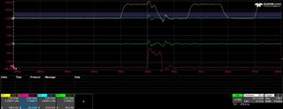
I also have the recordings in CSV files for the 4 channels (C1 = CLK, C2 = MISO, C3 = CS, C4 = MOSI) if that helps.

When I first observed this problem (before I had scope traces) I thought it always happened around 2048 (which is half of the 4096 12-bit ADC max range). In the attached JPGs the problem looks like the ADC trying to start with a 1 (implying ADC >= 2048) which would support the "it happens around MSB=1 (ADC approximately 2048)". However, further tests with a sawtooth in the range 0.5V..1V (so nowhere near 2048 ADC) also had issues. It might be a factor but not the full story.

I am using defaults for most of the registers, specifically CPOL/CPHA are both 0. Channels 1 and 3 are set to ANALOGUE INPUT with all others set as GPIO INPUT. When I used the NXP/TI development boards I had all channels set to 0V or 3V, except channel 3 which had the sawtooth.

During other tests I noticed the following

  • Erroneous channel number (usually double the required channel), i.e. channel 6 instead of 3.
  • Sometimes I also got channel 0 but less often than getting double the required channel.
  • I also did some READ, REGISTER, 0 and got back what looked like ADC readings (2 bytes of ADC/channel value then 0x00) rather than a register read (1 byte of register value, then 0x00 0x00).

In the READ, REGISTER, 0 returning an ADC reading I am guessing that the ADC did not interpret the command correctly so rejected it and therefore outputs the latest ADC reading. If the underlying problem is a clocking issue then this would make sense and is just the reverse of me seeing a doubled channel number.

Are you able to shed any light on this problem? Do the JPGs and CSV files help?

Thanks
Darren
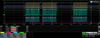
    Z2--got you 1--00001.csvZ3--got you 1--00001.csvZ4--got you 1--00001.csvZ1--got you 1--00001.csv

  • Hi Darren,

    When reading conversion data, a 20-bit wide SPI frame is used, where the first 12 bits are conversion data, the next 4-bits would be the appended channel ID bits in your case, then followed by four 0s. 

    The 24-bit SPI frame is used for device programming operations such as read and write registers. 

    Could this be contributing to the issue that you are seeing?

    Regards,
    Joel

  • I found the datasheets very confusing, for example section 8.3.12.2 mentions the existence SET BIT (0x18) and CLEAR BIT (0x20) but nothing else in datasheet shows how to use it. Is it a feature from another ADC chip that should have been removed from this datasheet or is the SET BIT/CLEAR BIT section missing from this datasheet?

    As to the 16-bit wide or 20-bit wide SPI frame issue...Section 8.3.9 mentions "12 SCLKs minimum. Remaining clocks optional." so I would expect 24 bit frames are OK. Interestingly the SDI line is not present in the diagram. Since SPI will always return MISO data from the ADC then if the previous command is a "READ, register, dummy" section 8.3.12.2.2 shows that the register value is returned in the first 8-bits, then 0s to pad out to the rest of the frame sent over MOSI. If the previous command is NOT a READ command then I am guessing that the ADC will always return the latest sampled 12-bit ADC value instead, followed by optional channel number or status, then 0s to pad out to the rest of the frame sent over MOSI. This is not explicitly mentioned, but would make common sense, an ADC that must return a value might as well return the latest ADC sample.

    Figure 34 in section 8.4.2 implies that ADC results are returned in a 24-bit frame (since the "Switch to AINz" is a WRITE, CHANNEL_SEL, z sequence). This is what I am using "WRITE, CHANNEL_SEL, 3" then another "WRITE, register, refresh_value". We need to refresh the ADC registers due to our design/code standards.

    Therefore, I don't think sending a 20-bit wide SPI frame instead of our 24-bit frame will help. I guess that would have to be a "NO-OPERATION, 0x00, 0x0" (the last part being 4-bits to make the 20-bit frame).

    I also didn't mention that I am running with CONV_MODE = 0, SEQ_MODE = 0, OSC_SEL = 0, CLK_DIV = 0. I am also running at 8MHz bit rate, but I saw the same issues at slower rates.

    I am now trying to repeat the setup and oscilloscope trace on the NXP/TI development board combination.

  • Hi Darren,

    It looks like the first two images you included are identical. If there was supposed to be another image here, and you think it might be helpful, can you include it in your response?

    The set bit and clear bit commands will work exactly the same as the single register write command. The only difference would be the opcode provided on the first 8 bits on SDI. The only difference of course would be that a set bit command will set high the bits specified in the 8-bit data field of SDI without modifying other bits. The clear bit command will set low the bits specified in the 8-bit data field of SDI without modifying other bits. This would be worthwhile to clarify in the datasheet though, and I'll leave it as a suggestion!

    It appears that you are using the device correctly, and yes, you can give the device a 24-bit command while getting the latest conversion data. 

    All the above that you have mentioned does lead me to believe this is most likely a clocking issue. The issue of channel number doubling could then be due to an unwanted bit shift (0011 becoming 0110). From a glance, it does look like you are meeting the minimum timing requirements. My first though was that CS is not being held high long enough before the erroneous data, but it seems to be ~250ns. Can you confirm this? Could you also confirm the frequency that SCLK is running at during conversion? 

    If it turns out the clocking is not an issue, then it could possibly be an issue with the individual device you are using. If adjusting timing doesn't work, would you be able to perform a direct swap with another device?

    Regards,
    Joel

  • The 2 JPGs were identical (my mistake on the scope).

    I have replicated the problem on the NXP dev board talking to the TI dev board. However, current thinking is that it MIGHT be a test setup issue, we are doing more testing.

    Currently we have scope traces showing 6 consecutive bytes from 2 messages with an interesting MISO mini-spike. We are not sure if it is due to the clock or grounding or something else, further testing is aimed at resolving this.

    The 6 figures below show the same 6 separate SPI messages along the trace picutre's top row with a different single byte zoomed out on the bottom row. The input is an increasing sawtooth so we should be seeing increasing ADC readings on channel 3. The returned readings are...

    • Message 1 = 0x7b0 channel 3
    • Message 2 = 0x7b6 channel 3
    • Message 3 = 0x7b1 channel 3 (value a little less than previous - probably within noise margins of readings)
    • Message 4 = 0x7b4 channel 6 (wrong channel, but ADC reading seems OK)
    • Message 5 = 0xff0 channel 0 (oh dear)
    • Message 6 = 0x7ae channel 6 (wrong, but ADC reading seems OK)

    CS = blue

    CLK = yellow

    MOSI = green

    MISO = red

    CPOL = 0, CPHA = 0

    Bit rate = 1MHz (1us per bit)

    When CLK is low  MISO prepares the next bit ready for rising edge.

    Figure 1

    Message 4 = 0x7b4 channel 6 (wrong channel, but ADC reading seems OK)

    Byte 1 = 0x7b (all looks normal)

    There is a little ringing at each CLK change.

    Figure 2

    Message 4 = 0x7b4 channel 6 (wrong channel, but ADC reading seems OK)

    Byte 2 = 0x46 (something is amiss, should be channel 3)

    Here we have a minor spike on MISO near the -72.205us marker. Interestingly, if the ADC was trying to send a 1 here and the other bits were then shifted down we would have had 0x53 which would have meant 0x7b5 on channel 3, much more meaningful.

    It is here that the ADC reading is going wrong and affects my project. This is why I turned on the "output channel number" feature. In this particular case though the reading 0x7b4 is quite reasonable as it is the LS-bit of the 12-bit ADC value. However, if the minor spike trying to drive a 1 but becoming a 0 occurs on the first byte then it can become the MS-bit of the ADC value and turn a 0x800 into an 0x000 which is a major alteration in value.

    The ringing on all of the other CLK changes are consistent with the first picture.

    Figure 3

    Message 4 = 0x7b4 channel 6 (wrong channel, but ADC reading seems OK)

    Byte 3 = 0x00 (all seems OK)

    The ringing on all of the CLK changes are consistent with the first picture.

    Figure 4

    Message 5 = 0xff0 channel 0 (oh dear)

    Byte 1 = 0xff (oh dear)

    Has the ADC got completely lost in its state machine? Not sure what is going on here. Is this a consequence of the previous errors? Could the ADC be responding to the previous message 4 command 0x081103 but mis-interpreting it as 0x101103 or 0x102206 or some other command (missing the first bit at the start of the MOSI command so it all shifts left one bit)? If it thought it was doing an 0x10 READ instead of 0x08 WRITE then it would make sense for the ADC to return the register value, but which register was it? The returned value is 0xFF which is not valid for CHANNEL_SEL (0x11) or EVENT_COUNT_CH0 (0x22).

    The ringing on all of the CLK changes are consistent with the first picture.

    Figure 5

    Message 5 = 0xff0 channel 0 (oh dear)

    Byte 2 = 0x00 (oh dear)

    Again, not sure here. See figure 4 comments.

    The ringing on all of the CLK changes are consistent with the first picture.

    Figure 6

    Message 5 = 0xff0 channel 0 (oh dear)

    Byte 3 = 0x00 (normal)

    Are we back in sync again? The next message 6 (in the top row of every picture) shows sensible ADC value but wrong channel 6 again.

    The ringing on all of the CLK changes are consistent with the first picture.

    I will make another post with my setup as adding more JPGs seemed to mess things up a bit.

  • After this test I tried to simplify the number of wires and grounds on my setup. I removed 3 scope probes, leaving just MISO and set a trigger to capture the mini-spike (HIGH for duration less than 120ns - remember a single bit was 1us).

    With the setup pictures here I didn't see any issue, but if I changed the CLK (direct between NXP and TI boards) into 2 wires in one of the white strips then my code went funny again (waiting for BOR to be set to a 1 after an ADC software reset WRITE, CFG, 0x01). This is what I meant about further grounding and clocking investigations. Whilst this might indicate a poor setup electrically we did see the issues on our production card as well. Further investigation is taking place.

    That's me done until I can complete our other investigations.

    Is there anything in all of this that suggests an issue with the ADC or is it purely grounding/clocking wiring?

    Thanks

    Darren

  • A slight update, pictures will come tomorrow.

    With have tidied up the wiring even more.

    Running at 8 MHz I still see an issue with the mini-spike to a 1. Sometimes the ADC is trying to set a 1 (ready for the next bit?) whilst the CLK is HIGH. Normally it prepares the next bit value after the falling edge of CLK. We have pictures of it doing this just before the end of the HIGH period of the CLK. This must be wrong,

    Interestingly running at 4 MHz the problem seems to have gone away, but 4 MHz is on our limits of acceptable SPI bus speed.

    I am running the 4 MHz overnight, although I expect it to still be running in the morning. At 8 MHz it was failing with these spurious mini-spikes within seconds.

    More details to follow tomorrow, with pictures.

    Darren

  • Hi Darren,

    Thank you for preempting the next concerns and questions that I would have had. 

    Since some of the issues are sorted out by modifying the test setup, this would point to that being the main culprit. The long jumper wires and breadboard connections are also likely to contribute overall to the issues we're seeing, as they contribute to higher resistances and parasitic capacitance.

    Because of this, the first step I would take is in optimizing this test setup. This means reducing the length of the conductors, avoiding external connections such as the breadboard power rails, using probes that won't load the circuit, and using a short ground connector for the oscilloscope probe.

    While I'm still not sure what the exact issue is, the device trying to drive a 1 on the third falling edge in figure 2 does seem also seem to indicate a possible issue with the device, but from your description, it does seem to occur across multiple devices, correct? It is unlikely that the same identical issue will occur across more than 1 device. In the same place, I am also noticing that the MOSI line drops down quite a bit as well. Do you have any other knowledge on what could be causing this condition? 

    Can you tell me a little bit more of the issues you're seeing in the production card? What connection are there from the controller to the ADC in this case?

    Regards,
    Joel

  • Sorry, but here comes another long essay!

    I just found out that another project has said that they have seen erroneous ADC values of 0.

    My issue started because I wanted to synchronise the ADS7038 ADC sample with an internal ADC in our NXP chip. I wanted to say "go SPI, go internal ADC" but the internal ADC would start sampling straight away whilst the ADS7038 sample would only happen once some part of the 2 command SPI message had been received. My messages are always "WRITE, CHANNEL_SEL, 0x03", followed by "WRITE, different_register_each_message, refresh_the_register_value". The 2nd command periodically refreshes all ADS7038 registers and also returns the ADC reading from the 1st command.

    I am not sure of the exact point when the input channel is aquired as I find the datasheet hard to read in this regard. From figure 1 "Conversion Cycle Timing" my understanding (guess) is that when CS goes LOW (to start receiving the 1st command) it "acquires" the channel 3 sample. Note, in my setup the 1st bit is sent 250ns after CS goes low. The acquisition time can be programmed and I am using OSC_SEL=0, CLK_DIV=0 to give a sample ("aquire" and "convert") every 1us. Since tCYCLE = tACQ + tCONV and tCONV is fixed at 600ns this means tAQC = 400ns. Since I am running SPI at 8MHz it takes 3us to send a single command. Therefore, the ADC has "acquired" the sample long before the end of the 1st command. The figure then implies it is converted on CS rising HIGH, i.e. at the end of the 1st command. After the last bit of the 1st command is sent I wait 125ns before raising CS HIGH. I then wait 250ns before sending the 2nd command. This means that the ADC channel is then "converted" at the start of the 250ns wait period. Since the "convert" takes 600ns there is another 350ns before the sample is ready. However, after the 250ns wait period (with CS high) I drive it low for the start of the 2nd command. This should start a new "aquire" but we are still doing a "convert". This clearly doesn't make sense. What is really going on? If you can tell exactly when/how the acquisition and sampling occur in my scenario that would be great.

    Anyway, we are driving our NXP chip via a PDB (programmable delay block) which has a "delay timer" that can be set to start the internal ADC sampling in "xxx ns" time. I was trying to find the correct value of this delay timer to synchronise both samples.

    To achieve this our hardware team (I am a software engineer) added a BNC connector and wiring direct to the ADC input channel to feed in my incrementing sawtooth input. They also disconnected the circuitry that feeds the ADC with our real signal. The idea was to set the "delay timer" to 100, take the internal ADC and ADS7038 reading and see who had the highest value which would indicate this was the later reading. Adjust the timer accordingly (lower if internal ADC was later, higher if ADS7038 was later). Repeat the test and adjust again. Repeat until both readings were roughly the same (I realise noise would mean they are never identical, but close enough).

    It was during this testing that my sawtooth went through expected ADC readings in the range 200 to 2800. Whilst debugging I saw readings close to 0, others close to 4095 and others about 3000, all of which were unexpected, out of range, i.e. wrong. Naturally I confirmed, with another scope, that the 200..2800 was what was truly being fed into my card. At this point I concluded an issue with the ADC. Since continuing this investigation and also in this forum post I obviously had not accounted for potential issues with the test wiring added to our card. I am now updating our production card code to record "too low" and "too high" ADC values and feed in a known static value (the nature of the true reading makes it hard to realistically replicate a sawtooth). I will run this new code on a card with no modified wiring alongside my originally modified wiring card and see if I get any "too low" or "too high" values. This should be able to determine whether the original test wiring is the culprit and this has all been a red-herring (although I learnt a few more things about this ADC along the way).

    I am still awaiting the pictures of our cleaned up dev board setup with shorter wires and better connectors. We do have some active probes on site that we could replace the original scope probes with at a later date (they are currently in use by someone else).

    I am attaching 4 scope traces that show something interesting on our cleaned up dev board. Again we have the mini-spike of a 1 trying to be driven by the ADC on MISO. However, this time it happens before the trailing edge of the clock. The zoomed in screenshots clearly(?) show that MISO is being driven first and the other 3 signals are ringing as a response to MISO, but then I am a software guy, not a hardware engineer.

    Thanks

    Darren

  • Hi Darren,

    For all intents and purposes, t_CONV lasts as long as CS is high, and t_ACQ lasts as long as CS is low. To achieve max throughput of 1MSPS (cycle time of 1us), with a max t_CONV of 600ns, this leaves 400ns for t_ACQ. During this 400ns, 24 clock cycles must occur for device programming commands, making this 16.666ns per clock cycle. This translates to a the specified maximum SCLK frequency of 60MHz. 

    What the t_CONV max specification then is really telling us is the minimum amount of time that CS must be high so as to not interrupt the conversion process; 600ns. 

    The acquisition time can be programmed and I am using OSC_SEL=0, CLK_DIV=0 to give a sample ("aquire" and "convert") every 1us. Since tCYCLE = tACQ + tCONV and tCONV is fixed at 600ns this means tAQC = 400ns. Since I am running SPI at 8MHz it takes 3us to send a single command. Therefore, the ADC has "acquired" the sample long before the end of the 1st command.

    This part above I'll need some help understanding. I think it would help to clarify that the OSC_SEL and CLK_DIV fields are really only for use with the internal averaging filter. While not using the internal averaging filter, everything will be controlled by the SCLK you provide from the controller. The phrasing in the datasheet can definitely be clearer here, and I'll make sure to make note of it for the next datasheet revision.

    Essentially what I'm saying is that the sampling rate you are getting is not actually dependent on the OSC_SEL and CLK_DIV fields, but on the SCLK frequency provided and the rising and falling of CS. The real t_CYCLE will then be however long you keep CS high (t_CONV), plus how long it takes for you to provide 24 SCLK cycles (t_ACQ). It should also be mentioned that t_CONV will be fixed at a maximum of 600ns (though the device won't enter acquisition as long as CS is high), but t_ACQ will change depending on how long CS is held low for. 

    With that, this leads me to believe that the issue is that CS is not being held long enough. Make sure that at a minimum, it is being held high for 600ns. Thank you for explicitly pointing this out to me, as I missed it when doing some rough calculations with my screen pixels. Anything shorter than 600ns could interrupt the completion of the conversion phase, which I believe is happening here.

    Regards,
    Joel

  • Thanks for the clarification of the acquisition and conversion process. Am I correct in the following...

    • While command "WRITE, register, value" is being transmitted CS is LOW so the currently selected channel is acquired. The acquisition takes as long as the command is being transmitted. So in my case, at 8MHz, the acquisition takes (3us + delay from CS low to first bit sent + delay from last bit sent to CS high).
    • At the end of the command CS is set HIGH and must remain HIGH for at least 600ns.
    • On the next command the ADC outputs the reading that was acquired at the time the "WRITE, register, value" was being transmitted.

    Therefore, to summarise

    • To use a single channel (which has already been defined by WRITE, CHANNEL_SEL, channel), the sequence would be
      • 1) WRITE, register, value
      • 2) WRITE, register-2, value-2
      • The return value from the 2nd message will be the ADC value acquired beginning from the start of the 1st message from the previously defined single channel
      • The register and register-2 can be CHANNEL_SEL with the single channel, but neither commands are required to be this register
    • To use more than one channel the sequence would be
      • 1) WRITE, CHANNEL_SEL, new_channel
      • 2) WRITE, register, value
      • 3) WRITE, register-2, value-2
      • The return value from the 3rd message will be the ADC value acquired beginning from the start of the 2nd message from the new channel

    I made a single setting change of DBT (delay between transfers, i.e. minimum time CS is HIGH) from 250ns to 600ns and the readings no longer failed. I reset back to 250ns and I got failed readings. This might be my main issue. I inherited the initialisation code from someone else Slight smile. I seem to inadvertently latched onto OSC_SEL and CLK_DIV but I knew we were trying to drive the reading as fast as possible. The inherited code just had the OPMODE_CFG register set to 0 with no comments describing the reason for each bit, e.g. a comment "OSC_SEL = don't care (averaging mode not used)" might have been useful. I try and say why each bit is set the way it is, especially on the "don't care" values.

    By failed readings I mean ADC values that fall outside the expected range of my sawtooth input.

    I then set DBT to 75ns as a quick test, since, if 250ns is too fast (needs 600ns) then 75ns would be even more too fast (poor grammar but you get the point).

    Weirdly this value worked fine! I found lots of other small DBT settings that worked. There were 8 consecutive values of DBT that fail (17..24) with my inherited value of DBT = 18 being one of them! These values equate to "(<n> + 2) * 12.5ns [SPI input clock = 80 MHz, i.e. 1 clock tick = 12.5ns]" so CS is HIGH anywhere from 237.5ns..325ns. Values either side of this seemed to work (no failed readings).

    I then changed my sawtooth to a level voltage. Interestingly all 3 settings (75ns, 250ns, 600ns) worked.

    My thought on why we are getting invalid answers only sometimes is that the ADC is performing a halfway ladder check, i.e.  (input < AVDD / 2) and set bit 11 accordingly, then check (input < AVDD / 4) and set bit 10 accordingly, (input < AVDD / 8) and set bit 9 and so on. This would be the checks for converting a 0V input, other values would go down different ladder sequences. I don't think I have the correct wording but I am guessing you understand what I mean here. Anyway, with a 250ns delay (conversion time) I am guessing the ADC has correctly calculated the first <n> bits but as the CS is now low it has to return a value over SPI so it returns the <n> bits of the new reading and the remainder of the old reading, a half-new, half-old value. This is why I think the level voltage input, rather than the sawtooth, worked in all cases since the half-old bits were the same as the previous sample, but with rapidly changing bits in a sawtooth this half-and-half problem exhibited itself. Is this the reason? In the end we need to stick to 600ns to not interrupt this conversion process, but I am curious to find out the reason why 250ns worked most of the time. Did we interrupt it at precisely the wrong time, with other (still too early) times being OK?

    I think we might be getting to the end of this issue.

    So I have now changed the following, from the inherited code

    • SPI input clock changed from 40MHz to 80MHz to address the 45:55 duty cycle requirement (40MHz gave 3:2 duty cycle [3 HIGH, 2 LOW @ 25ns], 80MHz gives 1:1 duty cycle [5 HIGH, 5 LOW @ 12.5ns]).
    • DBT from 250ns to 600ns
    • Turn on reporting channel number (APPEND_STATUS = 01b) just because I can and I can always confirm we are reading channel 3

    I will add similar range checking code to our production card and run a soak test to see if these fix my problem. I will also inform the other project (that saw random 0 values) about the duty cycle and 600ns requirements.

    I am going on holiday next week for about a month so I might not respond to further comments, however, I have some colleagues who will be keeping an eye on this thread.

    Hopefully I will then be able to mark this as resolved.

    Darren

  • Hi Darren,

    I think you've got a clear understanding of this device down! 

    It is important to note that when programming the device to switch to a different channel, this channel's data will be output 2 conversion cycles afterwards. See the relevant figure below. So technically, the channel that was selected 2 cycles ago is being currently output on SDO. You understand this already, but I just wanted to provide you the visual that describes this. 

    It is interesting that a CS of 75ns still worked. It would be worthwhile to investigate whether this interface has a critical timing sections that must not be interrupted, and to what particular degree of error cutting the conversion short will produce. I think your justification does seem to make sense. If the conversion process is halted before the critical section, the successive-approximation register might maintain the previous conversion, or change some parts of it. If it is halted during the critical section however, after the previous conversion has been discarded, it could yield a completely wrong result. I would also like to determine what the cause of the spike on MISO is caused by.

    The answer to the above might be out of my realm of expertise, but I'm definitely interested on the explanation as well. Maybe someone on the design team could shed some light on this. I hope this suggestion is able to fix the problem though! 

    Regards,
    Joel

  • Part Number: ADS7038

    Tool/software:

    This is an addendum to the thread https://e2e.ti.com/support/data-converters-group/data-converters/f/data-converters-forum/1400970/ads7038-erroneous-adc-values-being-returned

    Whilst I was on holiday another engineer took my code and showed that we had no further issues once we had changed our ADC configuration to use

    • 50:50 duty cycle on the clock (we originally had 40:60) – although I doubt this was the real cause of our issues
    • Delay between transfers set to 600ns (end of one 24-byte message to the start of the next [end-to-start]). Your datasheet says we only need 600ns delay between start of one 24-byte message and the start of another [start-to-start] but our SPI register settings uses [end-to-start] so we are keeping it simple. Using this end-to-start approach just wastes a bit of time but that doesn’t matter in our case and it easily shows we meet the 600ns minimum time.

    Whilst all of the timings are mentioned in the datasheet I will say that I found the datasheet quite confusing to read and could certainly do with a tidy up.

    This means that the thread can be marked as SOLVED

    Darren