This thread has been locked.

If you have a related question, please click the "Ask a related question" button in the top right corner. The newly created question will be automatically linked to this question.

ADS1299EEGFE-PDK: ADS1299EEGFE-PDK

Part Number: ADS1299EEGFE-PDK
Other Parts Discussed in Thread: ADS1299

Tool/software:

Hi,

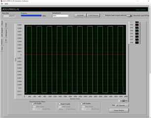
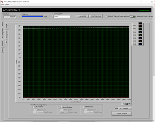
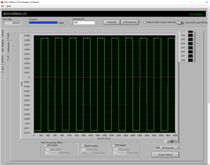
When I was testing ADS1299, I found that the signal was offset through the GUI. I used the waveform generator to generate a square wave with an amplitude of 20mV and a frequency of 10Hz, as shown in the figure.

But the waveform I observe through the GUI, seems to be shifted downward by 1.5mV.

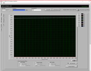
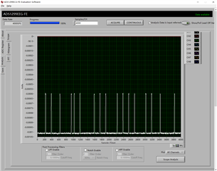
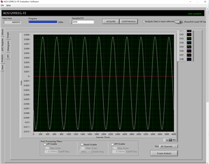
In addition, I also used a sine wave of the same amplitude for testing, and there was still a 1.5mV downward offset.

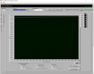
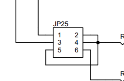
I used a waveform generator to generate an ARB wave, but there is still a 2mV downward offset. I would like to know how to eliminate it? The way I connected it was to use channel 1, connect the positive end of channel 1 to the positive output of the waveform generator, and the negative end of channel 1 to the negative end of the waveform generator and the ground end of the JP5 pin on the ADS1299 board.

Many thanks 

Junzhe

  • Hello Junzhe,

    Thank you for your post.

    The typical offset voltage for the ADS1299 IC itself is much less than what you have measured (typically 60 µV @ Gain = 12). You should see a much smaller offset if you configure the channel to use the internal square wave test signal.

    The majority of the offset voltage is likely coming from the single-ended connection of your function generator to the channel input. You can calibrate the offset voltage in post processing. One test would be to connect your function generator but disable the output. Then, record the average DC output from the ADC channel and store in as your offset calibration value.

    Regards,

    Ryan

  • Hi Ryan, 

    Thank you for your answer. I control the function generator to output a 10Hz, ±10mV square wave signal, as shown in the figure. You can see that there is an error of about 1.5mV, as I mentioned before.

    I then turn off the function generator output, but keep it connected to the ADS1299, and I measure the offset. But what confused me is that every time I run a test, the value goes up and finally stabilizes at around 2.45V. But I don't think 2.45V is a reasonable answer. 

    In addition, in each test, I placed all jumpers on JP25 (1-2, 3-4, 5-6) as the default settings.

    I want to know if my connection settings are correct. If so, I think simply turning off the function generator to measure the offset is incorrect.

    In addition, I would like to know, if measuring an unknown signal, how can we determine whether the measured value deviates from the true value? Is it necessary to introduce INA between the ads1299 and the object being measured to eliminate potential errors?

    Many thanks

    Junzhe

  • Are you powering off the function generator, or simply disabling the output waveform (the latter was my intention). If the equipment is completely powered off, then the inputs to the ADS1299 channel are likely floating, which is why you see the results drifting over time. Try only disabling the function generator output, or remove the function generator and just short the INxP and INxN inputs as close to the external source connection as possible. This will at least allow you to calibrate the offset in the PCB signal path.

    Regards,

    Ryan

  • Hi Ryan,

    I disabled the output waveform of the function generator, and these plots were got under this circumstance. Which makes me confused. I haven’t try to just short the INxP and INxX. I will try it and see what will happen.

    Many thanks 

    Junzhe

  • Hi Ryan,

    I short connect the IN1P and IN1N and get the waveform like this.  It seems that the waveform generally maintains an amplitude of 1mV, but there is still some gap with the results I observed before.

    Many thanks 

    Junzhe

  • Hi Junzhe,

    Is this capture taken with J6 pins 34 and 36 shorted together? I would not expect to see such glitches in the output. Simply short the two pins, tie to a common-mode voltage (i.e. mid-supply), and configure the channel mux for normal electrode input. Nothing else should be connected to the input.

    Regards,

    Ryan

  • Hi Ryan,

    This is the data I measured after shorting pins 34 and 36 of J6. But I didn't connect them to the common-mode voltage. Maybe that's the problem. What terminal can I get the common-mode voltage from?

    Many thanks

    Junzhe

  • You can use any GND test point as mid-supply if you are using ±2.5V supplies.

    Regards,

    Ryan

  • Hi Ryan,

    I shorted IN1N and IN1P and connected them to AGND through one terminal of JP5. This is the waveform I measured.

    My PGA gain is set to 1 at this time. According to the instructions in the data sheet, the offset should be about 600uV, which is reasonable.

    However, the square wave signal I measured before has a deviation of 1.5mV from the actual value, which still confused me. I removed all jumpers on JP25. I don't know where the offset will be introduced again.

    Many thanks

    Junzhe