This thread has been locked.

If you have a related question, please click the "Ask a related question" button in the top right corner. The newly created question will be automatically linked to this question.

ADC16DV160: ADC16DV160\ADS Simulation S-Parameter

Part Number: ADC16DV160

Tool/software:

Dear Team,

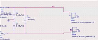
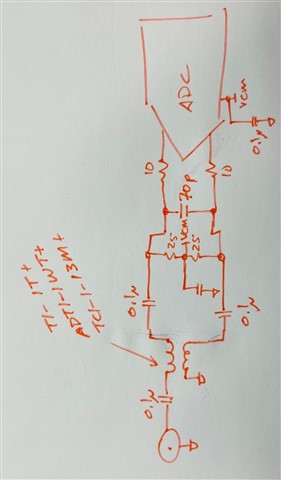
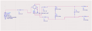
We are planning to use ADC16DV160 with transformer coupled front end design. We got S1P file for ADC from TI query.

But we are having issues during ADC simulation load impedance port assignment. ADC16DV160 have P & N pair signals for one channel but we only have one S1P file.

Q1) Can you confirm that this S1P file values obtained for ADC-(P or N) channel alone (or) ADC Total input impedance across P & N pins?

Q2) How to connect out front end circuit with ADC'S S-Parameter file?

Q3) Can you provide proper method for ADS simulation for ADC16DV160 termination?

We attached reference circuit for Reference.

Regards,

Esakki.

  • Hi Esakki,

    Can you please send me the link on where you downloaded the sparam files you are referencing?

    Also, if you let me know the following, I can help design a frontend for you.

    Bandwidth of the application.

    Passband flatness, ripple and flatness over the BW of the application

    min SNR/SFDR, minimum spec for noise and spurious

    Input Drive, of the input network if there is something driving that, signal generator, sensor or RF frontend circuit, what is the max signal gain from that previous stage that will connect into the primary of the transformer?

    Input Impedance, of the input network, previous stage that will connect into the primary of the transformer, what impedance does it need to have? 50ohms?

    This shouldn't be too point you in the right direction.

    Regards,

    Rob

  • Hi Rob,

    Thanks for getting back.

    Can you please send me the link on where you downloaded the sparam files you are referencing?

    I could not remember/ re-find, from where i have downloaded the File, kindly find the S parameter file in the attachment.(The File matches the S11 curve specified in Datasheet)

    Also, if you let me know the following, I can help design a frontend for you.

    My requirement below are as follows,

    Bandwidth: 50MHz

    Flatness: <1dB

    Input Impedance: 50ohms(from Signal Generator)

    Path Gain: NIL (Only path loss due to impedance matching network)

    Transformer Ratio: 1:1

    Insertion loss: <3dB

    Return Loss: <-10dB

    SNR @ -1dBFS: 80dBFs

    SFDR @ -1dBFS: >90dBc

    min SNR/SFDR, minimum spec for noise and spurious


    As i am new to ADC design, I thought only Insertion Loss and Return Loss could be simulated in ADS. Is it possible to simulate/ensure SNR/SFDR  specification?

    Thanks in-advance,

    Esakki

  • Hi Esakki,

    No you cannot simulate SNR/SFDR. With all that you outlined above, here is what I would recommend.

    Regards,

    Rob

  • Dear Rob,

    We were connected ADC front end simulations in ADS simulation as per attached image. For further return loss and Insertion loss measurement we need connect out front end circuitry with ADC input impedance.

    How to connect the ADC input impedance with IF front end circuitry?

    Please guide us for further process.

    Regards,

    Esakki.

  • Hi Esakki,

    I would use a parallel R||C value based on the input frequency of your application.

    This can be found on the S11 plot, in figure 31, on page 20, of the datasheet.

    Regards,

    Rob

  • Hi Rob,

    From the smith chart shown in S11 plot, in figure 31 of datasheet, we found that impedence of ADC input shall be

    28.325-j*274.979 Ohm. How to find the parallel R||C value for my 70MHz IF input frequency.

    Regards,

    Esakki.

  • Hi Esakki,

    I understand the issue.

    I am checking with design to see if they have the sparam files for figure 31. and the aggregate R||C values for the analog inputs.

    Otherwise, we need to do some iterative guesses to find the R||C based on the complex number you stated above.

    Regards,

    Rob

  • Hi Esakki,

    We don't have a copy of the Sparam data shown in Figure 31. I have checked all our archives.

    I also did a Google search on E2E and there is reference the link is broken or changed where the original application engineer that covered this device had a copy.

    How wide a frequency range do you need with your 70MHz IF? DC to 70MHz? or 70MHz +/-10MHz for example?

    Please advise, I may have an alternate approach that will work for you, if the BW is narrow.

    Regards,

    Rob

  • Dear Rob,

    Thanks for your reply. Our input frequency range will be 70MHz +/-12MHz.

    Fin - 70MHz +/-12MHz

    Please advise alternate option for ADS Simulation.

    Regards,

    Esakki

  • Hi Esakki,

    If you can estimate the R||C values, you can use this paper to help. it has an example to go by.

    Basically you will use a shunt inductor in front of the ADC's analog input to resonate away the internal C, this will create a natural BP filter at 70MHz.

    Regards,

    Rob

    https://www.analog.com/media/en/technical-documentation/app-notes/an-935.pdf

    https://www.mwrf.com/technologies/components/article/21840894/matching-an-adc-to-a-transformer