Other Parts Discussed in Thread: ADS114S06,
Tool/software:
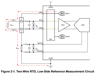
Hi. I have. 12 input configuration. I connect externally all inputs to AINCOM.
Internal 2.5V reference
I switch PMUX between 0 and 0x0B. Also Activate 500uA IDAC for the channel.
For inputs AIN0 - AIN7 I get ADC reading between 0 - 12. This is OK.
For inputs AIN8-AIN11 I get around 330. This is the problem.
If I don't activate IDAC, I get 0-12 ADC reading.
If I measure mV between input and AINCOM, it is 6mV when the channel is activated. All channels have 6mV, even the "good" channels. Doesn't seem to be the problem.
AIN8-AIN11 also happen to be optional GPIO, but it is in default state (analog input)
I checked SPI communication with logic analyzer and it is correct. Also made registers readback and registers as expected.
Could you help me understand, what is wrong with channels 8-11? I have 6 such boards and all behave the same. I seems to be some configuration issue.
Initial configuration:
const uint8_t ADS114_S08B_init_commands[] = {
0x03, //starting address
ADS_DELAY_14 + ADS_PGA_BYPASS + ADS_GAIN_1, //must be delay 14 for xx08B chip
ADS_FILTERTYPE_LL + ADS_DR_50, //bit7 must be 0 and bit 4 1 for xx08B chip
ADS_REFP_BYP_ENABLE + ADS_REFN_BYP_ENABLE + ADS_REFSEL_INT + ADS_REFINT_ON_ALWAYS,
ADS_IDACMAG_500, //7:4 must be zero for xB chip
ADS_IDAC2_OFF + ADS_IDAC1_OFF,
0, //VBIAS control
0, //Sys control. 1:0 must be 0 for xB chip
};
Channel switching commands:
SPI1_ByteWrite(0x40 + INPMUX_ADDR_MASK); //WREG command with starting address
SPI1_ByteWrite(6); //data length minus 1
SPI1_ByteWrite((Ch_no << 4) + ADS_N_AINCOM);
SPI1_ByteWrite(ADS_DELAY_14 + ADS_PGA_BYPASS + ADS_GAIN_1); //must be delay 14 for xx08B chip
SPI1_ByteWrite(ADS_FILTERTYPE_LL + ADS_DR_50); //bit7 must be 0 and bit 4 1 for xx08B chip
SPI1_ByteWrite(ADS_REFP_BYP_ENABLE + ADS_REFN_BYP_ENABLE + ADS_REFSEL_INT + ADS_REFINT_ON_ALWAYS);
SPI1_ByteWrite(ADS_IDACMAG_500); //7:4 must be zero for xB chip
SPI1_ByteWrite(ADS_IDAC2_OFF + Ch_no); //
SPI1_ByteWrite(ADS_VBIAS_LVL_DIV2 + 0); //Vbias