This thread has been locked.

If you have a related question, please click the "Ask a related question" button in the top right corner. The newly created question will be automatically linked to this question.

Excess THD in DAC8822 circuit used as audio DAC

Part Number: DAC8822
Other Parts Discussed in Thread: OPA1652, OPA1602, , BUF634, TINA-TI, OPA1612, OPA1656, OPA1642, DAC11001B

Tool/software:

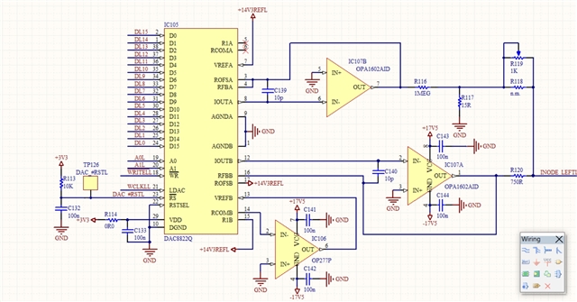
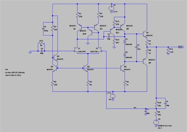
Hello, I'm using the DAC 8822 for a high resolution audio application as in the attached schematic. The 8822 is driven by an FPGA and the output of the circuit in the attached schematic is connected to the inverting input of an opamp used as inverting summer. While I reached the goals in terms of resolution, sampling frequency and SNR, the THD+N is much higher than expected. Please note that I minimized the major zero-crossing glitch by an auxiliary circuit, residual glitch spurious are well below the THD harmonics.

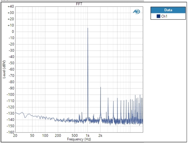
One cause I found for the excess THD was the limited GBW of the opamp initially used as I/V converter out of the 8822 (OPA1652). After replacing it with an OPA1602, I got a 6dB reduction of the THD. In order to check for need for further GBW, I reduced the VREF value, expecting even further THD reduction, but this didn't happen, therefore I guess the OPA1602 is ok.

THD @ 0dBFS out of the DAC circuit is now 0.002%, my goal is about 20dB less. The strange thing is that the THD out of IC107A ("coarse" DAC) is exactally same. I was expecting that the second DAC ("fine" DAC), which I use to "refine" the waveform of the first DAC (which works, as when I check the waveform @ -91dB, I still see a nice sinewave with 1% THD+N instead of a gross 1-LSBpp squarewave), helped to keep THD lower, but this doesn't happen.

Therefore I think the problem is mainly related to the first DAC. Is there any practical way to reduce the first ("gross") DAC THD? Is this related to some parameter like bipolar zero error, full-scale error or the like?

Thank you for your help.

  • Hi Fernando, 

    You are using channel B of the DAC8822 as a coarse DAC? And I assume this is what you mean by first DAC. Do you mean you are not using the lower bits to make larger code steps, and effectively a larger LSB size? This is what is reducing the THD of that channel. I assume channel A is the fine DAC and you are using the full 16-bit resolution? How are you using this to refine the first DAC?

    What sample rate are you using? And how many samples per period? 

    Best,

    Katlynne Jones

  • Hello Katlynne,

    thank you for your reply and please apologize for being not very clear. Yes, I use DAC B as "coarse" DAC, feeding it with the upper word of my 32-bit samples. The lower word is sent to DAC A which is used as "fine" DAC: its output is divided by 65536 and summed to the "coarse" DAC output. I choose DAC B as "coarse" DAC because, according to the datasheet, it's slightly better than DAC A in terms of INL and DNL.

    This proves to work because, as I said, I can see a nice sinewave @ -90dBFS and even -112dB with a reasonable 6-12% THD+N which is partly due to noise, partly to glitches spurious and partly to real THD.

    What puzzles me is the THD+N of the resulting signal at high levels (0dBFS to -20/-30dBFS), which seems to be exactally same as the THD+N of the "coarse" DAC itself, as if the "fine" DAC was not giving any contribution.

    While waiting for USA to wake up (I'm in Italy) I did some more tests and researches on Internet. The THD is mostly 2nd and 3rd harmonics. It seems to be due to the I/V converter and not to the DAC itself and this could explain why the contribution of the "fine" DAC is not effective in reducing the distortion.

    Now I'm figuring out how to improve the performance of the I/V converter. Somebody developed discrete components low distortion I/V converters. This is viable, but I hope there's a way to design a better opamp-based I/V converter. Would adding an extra differential pair to drive the opamp's inputs (plus some compensation) to increase the gain help? Also, somebody suggests to include a high current driver (like a BUF634) in the opamp loop to increase GBW and reduce the output impedance, therefore reducing THD: would this work in your opinion?

    For the record: I drive the DAC with sampling rates 44.1kHz to 768kHz and performance (on a standard 20kHz bandwidth) doesn't depend on the sampling frequency.

    Kind regards,

    Marco (Fernando)

  • Hi Marco,

    This is a very cool and interesting project.  I think you might be running into two different challenges here:

    1. Noise contribution: I think it is very important to differentiate between THD and THD+N.  I would expect your best case THD to be about equal to the theoretical best case dynamic range of the DAC.  There are few articles on how the quantization noise of a DAC is calculated, but approximate value is:

        DR(resolution) = 6.02dB(resolution)+1.76dB.

    So for your course DAC, we would expect about 98dB of THD.  The issue is that we have noise to consider as well.  So let's start by doing a noise analysis of just the course DAC.  

    The fine DAC would then need its own noise analysis.  I suspect that its total contribution to the output signal is actually less the that course DAC noise, or that the additive noise of the large capacitors is drowning the small-scale signal.

    2. I would also like to point out that combining DACs in this way is not as additive as you might think.  Scaling one DAC as you have done here does not really give you a 32-bit DAC.  In fact, if you were to look at the DC linearity, I would guess you have more of a ~17 to 18-bit DAC, maybe even <17-bit.  

    I think you should consider a few modifications to your design:

    1. Scale the reference of the DACA/fine DAC rather than scaling the output.  If you do the noise analysis you will a big contribution by these large values on the output.  

    2. Complete the noise analysis (TINA-TI is great for this as we have good noise models for the op amps you are using).  Don't forget to consider the noise of the reference.  If you have the instrumentation, you can try measuring these all individually to see if your simulations match the measured value.  Consider the current noise of the amplifiers as well voltage noise.

    3. Consider an architectural change.  Rather than a course/fine design, have you considered using the two DACs in parallel? This might only give you 17-bits of resolution, but it will be a reliable design and reduce noise.  You could potentially do a marginal scaling of the 2nd channel, course-ish to shoot for ~18+ bits.  This would require a bit of data manipulation.  

    Thanks,

    Paul

  • Hello Paul,

    thank you for your reply and suggestions. Attached please find the spectrum of the DAC total output @ 0dBFS. THD+N is, according to my AP analyzer, 93dB. You can see harmonics and residual spurious from code switching glitches. Just to check, I applied a steep 4.5kHz low-pass filter to remove the spurious and much of the noise while keeping the first 3 harmonics. The resulting increase in THD+N was about 1dB. The noise floor accounts for about 6.7uV. If harmonics and spurious were not there, the THD+N measurement should give about 109dB. To my knowledge, this means that my problem is indeed mainly THD and, to a lesser degree, noise or spurious. IMHO the question is: is the nonlinearity due to the DAC INL, bipolar zero error and full-scale error or is the I/V converter intrinsic THD? I have an opamp working with a 28.6Vpp swing on a 1500 Ohms resistor (the schematic in my first post says 750 Ohms, but I doubled it for a 6dB THD+N reduction. A further doubling actually increased the THD+N measure). I have the strong impression that the I/V converter needs improvement.

    Re. your suggestions about modding the DAC structure, I know that linearity is an issue below 100dB, nevertheless the signal is sooo nice compared to the 1-LSB square wave below -91dBFS, that I'd prefer to keep the "coarse" + "fine" arrangement. Yet, your suggestion to scale the "fine" DAC reference voltage and adjust its output attenuator accordingly might help and I'll try it.

    I'm surfing the 'net to find some suggestion to improve the I/V converter, but I mainly find DIY'ers forums discussing about discrete components, no feedback designs which might be ok, but I'd like something simpler to try.

    Would, using a high current, high bandwidth buffer in the opamp feedback loop to "isolate" its output from the input resistance and capacitance variations due to the DAC's output, help in your opinion?

    Thank you for all the support you'll want to give me!

    Best regards,

    Marco

  • Is it possible that you are seeing significant cross talk from your digital sources? If you take a look at zero scale tone, do you see significant harmonics/distortion at frequencies beyond ~3kHz? For example, continuously write the same code (0x5555, for example), and see what the FFT looks like.  If you see any spikes, they will likely have a different source.

    You can try a few different op amps for the I/V stage, like the OPA1656 or maybe the OPA1612.  These have different balances of current noise vs voltage noise.

    In addition, I dont see any capacitance on the VREF pins, which I highly recommend.  Does an FFT of your reference show similar spurs in the frequency domain? A mild LOW-PASS filter on the output might help as well against code to code glitch.

  • When I mute the data stream (fixed h8000) I don't see any spur in the FFT and the voltage is about 2uVrms.

    The partial schematic doesn't show it, but I placed 10uF ceramic X7R capacitors close to each REF pin of each DAC8822 IC.

    I checked the FFT of the ref voltage while the DACis converting 1kHz @ 0dBFS and I didn't see any appreciable 1kHz row.

    I tried OPA1652 and OPA1642 with worst results (higher THD), most probably due to slew operation because of too low GBW.

    I tried using a low pass filter for the glitches spurs but as far as they are in the passband the filter has no effect, unless an appreciabe IMD is present downsteram the I/V converter which moves higher frequency spurs into the passband... And this doesn't seem the case. With a periodic test wave, glitches have same period as the test signal and therefore produce spurs in passband, unless they are so short in duration that their harmonics are beyond 20kHz, which is also not the case, alas.

  • When you mute the datastream, are the digital lines still present? IE /LDAC and /WR?  What if you do ±1LSB tone?  Any change in noise?

  • Hello Paul,

    both /LDAC and /WR are always present. When I set the test signal level to -91dB the "coarse" DAC delivers 1 LSB and the noise floor doesn't rise appreciably.

    Yesterday I assembled a discrete-component FET-input (LSK170C) opamp. Please ignore C6. Standalone performance with 0dB gain inverting configuration (loaded with 1K5 as in the DAC board) driven with 10Vrms gave -140dB noise floor and 0.0002% THD+N, with as low as 0.00008% @ -2dB ref 10Vrms, very close to simulation data. As soon as I attached it to my test board, replacing the on-board OPA1602, THD jumped to 0.05%...

    Probably the breadboard and the wiring don't help, but this makes me think that the THD problem could be due to the abrupt input level change due to code switching... I don't know, maybe a small capacitor across the Iout pin of the 8822 an ground would help a little?

    The network at the bottom right simulates the DAC, while R11 is the resistor that goes to the output inverting adder.

  • Hi Marco,

    Code-to-code glitch is usually the primary contributor to distortion in our R-2R DACs.  (Which is why the track-and-hold circuit in the DAC11001B is capable).  A small capacitor should help, as it will help move the distortion our of the audible range. 

    Our output impedance is ~5kΩ, so a 1nF capacitor could be a good help (smaller might be needed at higher frequency output).  I also recommend a small resistor between the capacitor and the inverting input of the amp.

  • Hello Paul,

    thank you for your suggestions. Alas, they didn't work. I also tried to halve the reference voltage to check whether the THD is generated in the I/V converter opamp due to the large voltage swing. The result was actually an increase in the THD. I'm beginning to think that the problem is related to the DAC's DNL or full-scale error.

    I also checked the supplies and the reference voltage when the DAC is delivering 0dBFS: all three show the same harmonics and spurs content as the signal, but not the fundamental. Could it be a ground problem? My testboard has a solid ground plane on the bottom layer, all grounds refer to it, but not as a star.

  • Hi Marco,

    Does -1dBFS show to the same issue? How about -3dBFS? 

    I am surprised that the supplies would be showing the same harmonics.  The reference buffers should basically be driving a static load to ground.  What happens when you isolate reference for DACA? As you only buffer the reference for DACB, a glitch on the 14.3V reference would also cause a glitch on REFB.