A related question is a question created from another question. When the related question is created, it will be automatically linked to the original question.
However, I would also like to measure DC signals that do not change over time.
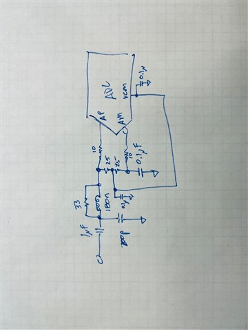
If I want to measure both DC and AC signals, would it be okay to remove the 1uF capacitor to make it 0Ω, and also to remove the 0.1uF capacitor near the 10Ω of AINM to make it 0Ω?
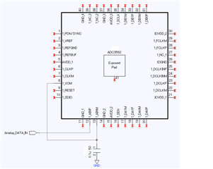
On page 8 of the datasheet, "Input full scale" is listed as 3.2V, but in the circuit on page 31 of the datasheet, the ADC3562 VCM (=0.95V) is connected to the FDA, so the scale at which the FDA can output a balanced signal seems to be just under 1.9V.
Is it correct to consider the differential full scale to be up to MAX 1.9V when sharing the VCM?
While the power shutdown is being performed at the PD terminal, is it correct to think that no common mode voltage (for example, the VCM default value Vss/2) is generated at the output and the output becomes a floating line?
I would appreciate a response as soon as possible.
In Pspice for TI, a common mode output voltage (=Vss/2) was generated even when PD was set to L. The system I am designing is configured so that the FDA power supply starts up earlier than the ADC3562 power supply, and if a voltage is generated at the output even when PD=L, the voltage will be applied to the input of the ADC3562, which is not powered on.The data sheet states that setting PD=L turns off the device and puts it into a no-signal current state, so it does not make sense that a common mode voltage is output when PD=L, and I would like to think that the Spice model is incorrect.
I cannot comment on the Pspice model. Hopefully the amplifier group can comment here.
Basically you have a cold sparring issue, where you will be applying voltage on the ADC pin, when the ADC is unpowered.
Do you need to DC couple the amp and ADC. If you truely don't need to sample the DC value, then you can use a DC blocking cap in series inbetween the two devices and this will remove the issue.
During power down the amplifier will go high impedance. If there is a signal present at the inputs it is possible you will still see some of that signal on the output as it feeds through the feedback network around the amplifier. However, the amount of signal that feeds through should be fairly small. I checked on the SPICE model and it does only show a small amount of feed-through. Could you check the text of the SPICE model file you are using and let me know what version it says? The latest is version 2.0.
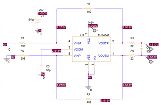
I've attached an image. The model number appears to be 2.0. As you can see in the image, even when PD is set to L, 2.5V is output to the output line. In your environment, does this mean that 2.5V is not output and it is in a high impedance state?
I think I should actually look at the actual measured values on an evaluation board, but I don't have an evaluation board to hand, so I would like to hear an official opinion.
This is the LVDS receiving terminal. Does it have a built-in 100 Ω resistor?
It seems common to attach 100 Ω to the receiving side, but I can't find any 100 Ω resistor in the sample circuit on the data sheet or the evaluation board circuit.
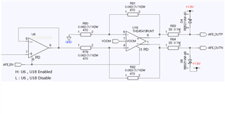
I have a question about the driver THS4541 for ADC3562.
Will the THS4541 shorten the life of the device if it repeatedly goes into an unbalanced circuit state where normal negative feedback does not work?
I have attached a circuit diagram.Two op-amps are connected with a common enable/disable line.When changing from L (disable) to H (enable), the THS4541 responds faster and is enabled first.At that time, the output of U6 is high impedance, so normal negative feedback does not work, and an unbalanced output that differs from theory is generated.The time is about 500ns.I am worried that repeating even 500ns many times will definitely shorten the life of the THS4541.
You would likely be okay with this scenario as long as the amplifier isn't overheating or drawing excessive current during the condition. If you want to be sure they start up at the same time, one easy fix would be to install a simple RC filter at the PD pin of the THS4541. You can tune the filter so that the enable signal is slowed down and the THS4541 starts up after the op-amp.


 Hi Rob, Thank you for your reply.