Tool/software:
Hello everybody,
I'm encountering an issue where the echo of the address is off by one when I send the reset command, and when configuring the PGA, INPMUX, and the Reference Voltage.This problem occurs every time with these three configurations and the one command. Additionally, the register value appears incorrect because the (LSB) is always set high. I've already used a logic analyzer to verify the signals, and the microcontroller is transmitting the correct signals. However, I'm getting ADC readings—for example, the ADC reports 1.948V while the measured value is 2.175V.
I am using the Arduino Framework and and Espressif ESP32-S3-DevKitC-1-N32R8V.
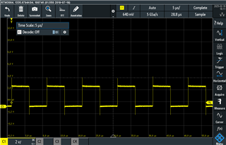
For the SPI Mode, I chose SPI_mode 1 (CPOL = 0, CPHA = 1) and the CLK speed of the SPI i tried various from 100kHz to 9 Mhz, and the output is still the same.
Here is the C++ Code Snippet:
ADS1261::ADS1261() : SPI_Instance(SPI0_Selector, (SPI_Chipselect)ADS1261_nCS, DataMode_1) {

    // Configure GPIOs
    pinMode(ADS1261_nReset, OUTPUT);
    pinMode(ADS1261_nPWDN, OUTPUT);
    pinMode(ADS1261_START, OUTPUT);
    pinMode(ADS1261_nCS, OUTPUT);
    pinMode(ADS1261_nDRDY, INPUT);

    digitalWrite(ADS1261_nReset, HIGH);  // Bring reset HIGH
    digitalWrite(ADS1261_nPWDN, HIGH);   // Power up ADC
    digitalWrite(ADS1261_nCS, LOW);      // Deselect ADC

    // Hardware Reset Sequence
    Serial.printf("Waiting for DRDY to be LOW\n");
    while(digitalRead(ADS1261_nDRDY) != HIGH){
        delayMicroseconds(100);
    }
    Serial.printf("DRDY is LOW\n");
    SendCommand(0xF5,0x00);
    digitalWrite(ADS1261_START, LOW);

    delay(60);
    Serial.println("ADS1261 Initialization Started...\n");

    bool Success = true;
    uint8_t Val = 0;

    Serial.println("Sending RESET command...\n");
    digitalWrite(ADS1261_nCS, LOW);
    delayMicroseconds(100);
    Success &= SendCommand(0x06, 0xAA);
    delayMicroseconds(300);

    // Unlock Registers
    SendCommand(0xF5,0x00);
    delayMicroseconds(300);
    Serial.println("Configuring ADC Registers...\n");

    /*
    MODE1:
    Currently in Chop mode and 17.8ms start delay
    also tested with Normal mode, Continous mode with 50 microseconds
    */
    Success &= SetRegister(0x03, 0x2D);  // tested with 0x10 and 0x2D
    delayMicroseconds(1000);
    GetRegister(0x03,&Val);
    Serial.println("---------------------------");
    Serial.printf("Read Value: 0x%x\n",Val);
    Serial.println("---------------------------");
    delayMicroseconds(100);
        /*
        PGA
        In Bypass mode
        Gain: 1
        */
    Success &= SetRegister(0x10, 0x00);
    delayMicroseconds(100);
    GetRegister(0x10,&Val);
    Serial.println("---------------------------");
    Serial.printf("Read Value: 0x%x\n",Val);
    Serial.println("---------------------------");
    delayMicroseconds(100);


    /*
    Internal Reference Voltage:
    Internal Reference enabled
    Internal ref. positive and negative
    */

    Success &= SetRegister(0x06, 0x10); //also tested with 0x15
    delayMicroseconds(100);
    GetRegister(0x06,&Val);
    Serial.println("---------------------------");
    Serial.printf("Read Value: 0x%x\n",Val);
    Serial.println("---------------------------");
    delayMicroseconds(2000);

    /*
    INPMUX:
    Postive Input: AIN0
    NegativeInput: AINCOM
    */
    Success &= SetRegister(0x11, 0x10);
    delayMicroseconds(100);
    GetRegister(0x11,&Val);
    Serial.println("---------------------------");
    Serial.printf("Read Value: 0x%x\n",Val);
    Serial.println("---------------------------");
    delayMicroseconds(100);

    digitalWrite(ADS1261_START, HIGH);

    Serial.println("Waiting for DRDY to be LOW...");
    while(digitalRead(ADS1261_nDRDY) != HIGH){
        delayMicroseconds(100);
    }
    Serial.println("DRDY is LOW");


    if (!Success) {
        Serial.println("Failed to initialize ADC registers!\n");
    } else {
        Serial.println("ADS1261 Initialization Successful!\n");
    }
}

bool ADS1261::SetRegister(uint8_t const Address, uint8_t const Value)
{
    const uint8_t WREGCommand = 0x40;
    return SendCommand(WREGCommand + (Address & 0x1F), Value); // taken from the example code of TI
}

bool ADS1261::SendCommand(uint8_t const Command, uint8_t const Data)
{
    const uint8_t BufferLen = 2;
    uint8_t const WriteBuffer[BufferLen] = {Command, Data};
    uint8_t ReadBuffer[BufferLen] = {0};


    delayMicroseconds(10);
    bool Success = SPI_Instance.ReadWrite(WriteBuffer, ReadBuffer, BufferLen);

    Serial.println("---------------------------------------------------------");
    Serial.printf("Sent Command: 0x%X 0x%X\n", WriteBuffer[0], WriteBuffer[1]);
    Serial.printf("Received Response: 0x%X 0x%X\n", ReadBuffer[0], ReadBuffer[1]);

    if(Command == 0x06){
        delay(10);
    }

    Success &= ReadBuffer[0] == 0xFF;
    Success &= ReadBuffer[1] == Command;

    if(!Success){
        Serial.printf("Failed to send command!\n");
        Serial.printf("Writebuffer: 0x%x 0x%x\n", WriteBuffer[0], WriteBuffer[1]);
        Serial.printf("ADC Command Buffer: 0x%x 0x%x\n", ReadBuffer[0], ReadBuffer[1]);
    }else{
        Serial.printf("Successful!\n");

    }
    Serial.println("---------------------------------------------------------");
    return Success;
}
And the Output:
Waiting for DRDY to be LOW
DRDY is LOW
---------------------------------------------------------
Sent Command: 0xF5 0x0
Received Response: 0xFF 0xF5
Successful!
---------------------------------------------------------
ADS1261 Initialization Started...

Sending RESET command...

---------------------------------------------------------
Sent Command: 0x6 0xAA
Received Response: 0xFF 0x7
Failed to send command!
Writebuffer: 0x6 0xaa
ADC Command Buffer: 0xff 0x7
---------------------------------------------------------
---------------------------------------------------------
Sent Command: 0xF5 0x0
Received Response: 0xFF 0xF5
Successful!
---------------------------------------------------------
Configuring ADC Registers...

---------------------------------------------------------
Sent Command: 0x43 0x2D
Received Response: 0xFF 0x43
Successful!
---------------------------------------------------------
---------------------------
Read Value: 0x2d
---------------------------
---------------------------------------------------------
Sent Command: 0x50 0x0
Received Response: 0xFF 0x51
Failed to send command!
Writebuffer: 0x50 0x0
ADC Command Buffer: 0xff 0x51
---------------------------------------------------------
---------------------------
Read Value: 0x1
---------------------------
---------------------------------------------------------
Sent Command: 0x46 0x10
Received Response: 0xFF 0x47
Failed to send command!
Writebuffer: 0x46 0x10
ADC Command Buffer: 0xff 0x47
---------------------------------------------------------
---------------------------
Read Value: 0x11
---------------------------
---------------------------------------------------------
Sent Command: 0x51 0x10
Received Response: 0xFF 0x51
Successful!
---------------------------------------------------------
---------------------------
Read Value: 0x11
---------------------------
Waiting for DRDY to be LOW...
DRDY is LOW
Failed to initialize ADC registers!