This thread has been locked.

If you have a related question, please click the "Ask a related question" button in the top right corner. The newly created question will be automatically linked to this question.

ADC12DJ5200RFEVM: ADC12DJ5200RFEVM + TSW14J58EVM

Part Number: ADC12DJ5200RFEVM
Other Parts Discussed in Thread: LMK04828, TSW14J58EVM, , TSW14J57EVM, TSW14J59EVM

Tool/software:

Dear Technical Support Team,

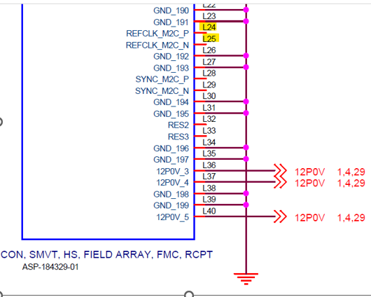
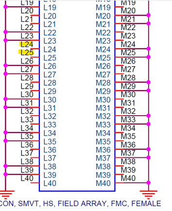
The FPGA_CLKA_FMC_N output(LMK04828) from the ADC12DJ5200RFEVM is input to L25 of the TSW14J58EVM, but in Rev. A, L25 is connected to GND.

Also, L24 and L25 seem to be unconnected for TSW14J57EVM and TSW14J59EVM.

Q1

Am I correct in recognizing that FPGA_CLKA_FMC_P and N from ADC12DJ5200RFEVM are not used especially in TSW?

Q2

My board silk has DC182_A10. Dose it mean Rev.A. Is it work with ADC12DJ5200RFEVM ?

According to this E2E, there is Rev.C board for  TSW14J58EVM 

TSW14J58EVM: Rev C board design files - Data converters forum - Data converters - TI E2E support forums

Best Regards,

ttd

TSW14J57EVM

■TSW14J59EVM

  • Ttd,

    The lanes are either grounded or not connected, therefore they don't connect to the fpga and cannot be used as a clock domain source. The fpga firmware has to use a different clock for application clock domain as a result. I don't know any of the details on this or how it was implemented in HSDC Pro but it should work for the TSW14J58 A10 board, which does mean Rev A (ver 10).