This thread has been locked.

If you have a related question, please click the "Ask a related question" button in the top right corner. The newly created question will be automatically linked to this question.

DAC81401: Issues in programming DAC

Part Number: DAC81401
Other Parts Discussed in Thread: DAC61401

Tool/software:

Hello!
I want to use DAC61401 for generating bipolar voltages for controlling the base voltage (Vb) of BJTs (both PNP and NPN). First, I started with verifying the working of the IC by itself on a breadboard. I use Arduino Uno R3 for the SPI communication. Please see the circuit diagram and arduino code attached.
Schematic_DAC61401_2025-03-20.pdf

DAC61401_control.zip

I could not get any voltage output (VOUT) or the read the internal reference (VREFIO). I tried the following:

1. Write 0x0A04 to reg 0x03 (suggested in the application section of datasheet)

2. Write 0x0000 to reg 0x04

3. Write 0xFFFE to reg 0x09

4. write 0x0005 to reg 0x0A

5. write 0x7FFF to reg 0x10

This should give output of 2.5V. But I could not get any output. When i did only step 1 and 2, still i could not measure VREFIO with a oscilloscope.

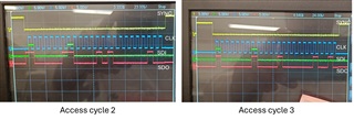
6. I verified that the SPI.transfer from arduino is working correctly. I could verify the transmitted bits are correct. I tried the 4 different SPI_MODEs but, no solution. 

7. I tried the SPI communication within the setup() function as well as loop() function of arduino.

8. I have used slower SPI at SPI_CLOCK_DIV128. Used at least 1ms delays after each 24-bit (8-bit reg + 16-bit word) transfers.

Please can you suggest what I am missing here. What modifications are necessary to the circuit or the code?

Thanks

Sagnik

  • Hi Sagnik, 

    Sanjay will review and get back with some suggestions soon. 

    Best,

    Katlynne Jones

  • Hi Sagnik,

    Please provide details for the following things - 
    1. Confirm if you are able to do the readback for any of the DAC registers i.e. DEVICE_ID pr SPICONFIG.
    2. If no, please share the SPI line (CS, SDIN, SCLK and SDO) scope snapshot for SPICONFIG (0x03) and GENCONFIG (0x04).
    3. And measure all the supply voltages on DAC power pins and let me know.

    Thanks,
    Sanjay

  • Hi Sanjay,

    I tried reading the DEVICEID register. I do not think I am getting the correct values. Based on the arduino code above, I am performing 3 SPI cycles as shown below. I am not writing the GENCONFIG reg.

      write_reg(0x03, 0x0A04); //SPI_CONFIG reg. 0x0A04 to enable SDO - update at rising CLK edge
      delay(1);
      //reading DEVICEID reg 0x01
      write_reg(0x81, 0x0000); // bit23 is 1 for READ command
      write_reg(0x81, 0x0000); // extra access cycle to read data
    Here are the screenshots from the oscilloscope of the 2nd and 3rd cycles:


    I have confirmed the first access cycle (not shown in image). The SDI is correct. It reads hex 030A04 (as expected)
    I checked the voltage supplied to the DAC. The VDD, IOVDD are at 5V. AVSS at -10V. AVDD at 10V.
    Please let me know what i am doing wrong.
    Sagnik
  • Hi Sagnik, 

    Thanks for the plots and additional details. Sanjay will review and get back to you soon. 

    Best,

    Katlynne Jones

  • Hi Sangik,

    SPI frame and power supply looks to be okay.
    Please try these two steps, and let me know the results.

    1, Write 0x0A04 to reg 0x03 and 0x0000 to reg 0x04, then read both of these addresses and report the readback data.
    2. Measure the VREFIO pin voltages and report the measured value, it should be 2.5V.

    If you are not getting the 2.5V, we need to have a live debug session to see what is going wrong here.

    Thanks,
    Sanjay