Other Parts Discussed in Thread: , ADS131M04
Tool/software:
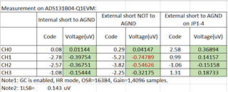
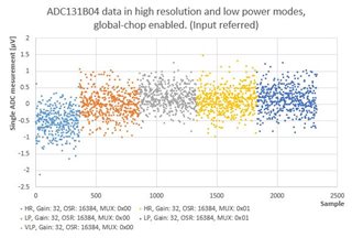
While testing the ADS131B04, different offset voltage levels on channel 1 were observed using different power modes while the input pins of channel 1 shorted externally.
Shorting channel 1 input via the MUX1 register shows an equal offset between both 'high resolution' and 'low power' power modes.
Global-chop was enabled in all modes so a typical offset of 0.4 µV was expected.
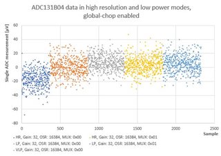
| AVG | STDEV | |
| Settings | [µV] | [µV] |
| HR, Gain: 32, OSR: 16384, MUX: 0x00 | -16.8 | 12.3 |
| LP, Gain: 32, OSR: 16384, MUX: 0x00 | 0.1 | 12.1 |
| VLP, Gain: 32, OSR: 16384, MUX: 0x00 | 7.2 | 10.6 |
| HR, Gain: 32, OSR: 16384, MUX: 0x01 | 4.0 | 11.5 |
| LP, Gain: 32, OSR: 16384, MUX: 0x01 | 4.7 | 11.9 |
Noise levels are close to the typical noise as specified for the ADS131B04-Q1.
What could be the reason that while the pins are shorted externally, the 'high resolution', 'low power' and 'very low power' modes show such different offset levels (resp. -16.8, 0.1 and 7.2 µV)?
EDIT 2025-04-24:
NOTE: To explain why the statement 'Noise levels are close to the typical noise as specified for the ADS131B04-Q1' is valid. The above values are internal on the ADC input, thus after programmable gain amplifier (PGA) and not on the ADS131B04 input pins. To get the 'input referred' value, the above values should be divided by 32.