This thread has been locked.

If you have a related question, please click the "Ask a related question" button in the top right corner. The newly created question will be automatically linked to this question.

ADS1261: Wokring with ADS1261 connected to ESP32

Part Number: ADS1261

Tool/software:

Hi everyone,

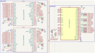
I’m working on a project where I designed a custom PCB that uses two ADS1261 ADCs to measure differential voltages between 16 electrodes. Here’s my setup:

  • Electrode Wiring:

    • ADS1261 #1: Electrode 1 to Electrode 10 are connected to AIN0–AIN9 respectively.

    • ADS1261 #2: Electrode 10 to Electrode 16 are connected to AIN0–AIN6, and Electrode 0 (the wrap-around electrode) is connected to AIN7.

  • ESP32 Connections:

    • Both ADS1261 devices share the same SPI bus. I have connected:

      • /DOUT_DRDY (from both ADCs) to MISO (GPIO19)

      • SCLK to GPIO18

      • DIN to MOSI (GPIO23)

    • Chip select pins are separate: ADC1 uses GPIO14 and ADC2 uses GPIO15.

    • Additionally, I have tied the START, /RESET, /PWDN, and /DRDY pins of both ADCs together (this might be an issue, but i think with the right addressing i can work around this).

  • Measurement Approach:

    • I plan to initialize both ADCs in parallel to run in 40 kSPS mode with a PGA gain of 64 (which suits my electrode voltage ranges) and to use the internal 2.5V reference. My idea was to send the same SPI commands to both devices simultaneously (by pulling both CS lines low at once) so they recieve the commands in parallel, and act accordingly in parallel.

    • After initialization, I would set the INPMUX (register 0x11) of both ADCs to the appropriate differential channels (e.g., AIN0–AIN1, AIN1–AIN2, …), then issue the START command in parallel. Once either device’s DRDY goes low, i would wait 1 uS, so i can ensure both ADCs finished sampling, and I would sequentially read each ADC’s conversion result by toggling their respective CS lines.

    • In testing, I tried to initialize one device and perform a differential measurement between AIN0 and AIN1, but the readout fails (always returning 0 or unexpected values).

  • Development Environment:

    • I am using the Arduino framework with PlatformIO for programming.

    • I have incorporated an ADS1261 driver (code from TI’s examples) and implemented the required HAL functions for my ESP32 (using SPI.transfer(), digitalWrite(), delay(), etc.).

My Specific Request:
I’m currently stuck at the very basic level:

  1. Initialization: How can I correctly initialize a single ADS1261 instance with the settings above (40 kSPS, PGA gain = 64, internal 2.5 V reference) using SPI-only control (ignoring /PWDN, /RESET, and START hardware pins)?

  2. Measurement: How should I correctly perform a single-shot differential measurement between AIN0 and AIN1 (i.e., set the INPMUX register properly, issue the START command, wait for DRDY, and then read the conversion data)?

If anyone has an ESP32-based driver example for the ADS1261—or can provide guidance on troubleshooting this one-device configuration—I’d really appreciate the help. Once I can successfully initialize one device and get a proper reading between AIN0 and AIN1, I can adapt the design for parallel operation with both ADCs.

Thanks in advance for your assistance!

Regards,
Balazs

  • Hi Balazs Hazi,

    Can you provide logic analyzer captures of the data communication during the initialization? Please include DIN, DOUT, SCLK, CS, DRDY, RESET, START, and PWDN

    -Bryan

  • Hi Bryan,

    I can't really povide logic analyzer captures of the mentioned lines, since currently i don't have a scope on me, later this week i will be able to use one hopefully, but i can describe what i implemented, and maybe we can figure out why it is not working properly. 

    Mainly im interestedin if this is the correct code for the case of an ESP32 controller, because i tried to implement the same initialization and measurement procedure as described in the datasheet, but had no success. This is what i implemented: pulling /RESET and /PWDN HIGH, checking if the /DRDY pin gets HIGH, check if START pin is HIGH, and if so set it to LOW so we work via SPI commands mainly. Also after this, i configure the ADS1261 by sending the commands: write register 0x06 with 0x10 to enable internal 2.5V reference, writing register 0x11 with 0x23 to set the input multiplexer to channels AIN1, AIN2, write register 0x10 with 0x06 to set PGA gain value to 64, write register 0x05 with 0x00 to disable crc, and finally send a start command 0x08 to start conversion.

    To read a conversion i use the following code: 

    int32_t readConversion()
        {
            uint8_t data[3];
            digitalWrite(ADC1_CS_PIN, LOW);
            SPI.transfer(OPCODE_RDATA);   // 0x12 command to read data
            SPI.transfer(0x00);           // Send 3 dummy bytes to clock out 3 data bytes (no status/CRC)
            data[0] = SPI.transfer(0x00);
            data[1] = SPI.transfer(0x00);
            data[2] = SPI.transfer(0x00);
            digitalWrite(ADC1_CS_PIN, HIGH);
            // Combine 24-bit data (ADS1261 outputs in binary two's complement)
            int32_t rawValue = ((int32_t)data[0] << 16) | ((int32_t)data[1] << 8) | data[2];
            // Sign-extend if negative:
            if (rawValue & 0x800000) { rawValue |= 0xFF000000; }
            return rawValue;
        }

    This code produces no valid readouts sadly, i don't know if the initialiozation fails, or the readout implementation is bad but it always returns the same values. My setup should produce samples of noise which i know is not ideal, but surely i shouldn't recieve the same measured values for each measurement. 

    This is the described initialization function: 
    void initilaize(void)
        {  
            pinMode(ADC1_CS_PIN, OUTPUT);
            pinMode(ADC2_CS_PIN, OUTPUT); // Currently no in use

            pinMode(ADC_RESET_PIN, OUTPUT);
            pinMode(ADC_START_PIN, OUTPUT);
            pinMode(ADC_PWDN_PIN, OUTPUT);
            pinMode(DRDY_PIN, INPUT_PULLUP); // Use pullup for DRDY
            delay(5);


            digitalWrite(ADC_RESET_PIN, HIGH);
            digitalWrite(ADC_PWDN_PIN, HIGH);

            delay(5);

            unsigned long start = millis();
            while(digitalRead(DRDY_PIN) != HIGH){
                if(millis() - start > 1000){
                    Serial.println("DRDY timeout during initialization...");
                    Serial.println("DRDY state:" + String(digitalRead(DRDY_PIN)));
                    start = millis();
                    //break;
                }
            }

            bool startHigh = digitalRead(ADC_START_PIN) == HIGH;

            if(startHigh)   // Or could send STOP command
            {
                Serial.println("Start pin was high pulling it low");
                digitalWrite(ADC_START_PIN, LOW);
            }

            // 2. Enable internal 2.5V reference and select it as reference source
            uint8_t refConfig = 0x10        // 0x10: enable internal reference
                            | 0x00          // 0x00: internal reference positive input
                            | 0x00;         // 0x00: internal reference negative input
            writeRegister(0x06, refConfig); // Write REF register (address 0x06) with value 0x10
            delay(20);  // Wait 20+ ms for internal reference to stabilize (required for accuracy)

            // 3. Configure input MUX for differential AIN1-AIN2
            uint8_t muxConfig = 0x20        // 0x20: positive input = AIN1
                            | 0x03;         // 0x03: negative input = AIN2
            writeRegister(0x11, muxConfig); // Write INPMUX register (address 0x11) with value 0x23
            // Now the ADC will measure the voltage difference V(AIN1) – V(AIN2) on each conversion

            // 4. Set PGA gain to 64
            uint8_t pgaConfig = 0x06;        // 0x06: PGA gain = 64 (binary 110)
            writeRegister(0x10, pgaConfig);  // Write PGA register (address 0x10)

            // 5. Set data rate to 40,000 SPS and choose filter (use Sinc1 for lowest latency)
            uint8_t mode0Config = 0x80        // 0x80: data rate = 40kSPS (max)
                                | 0x00;       // 0x00: Sinc1 filter (fastest settling)
            writeRegister(0x02, mode0Config); // Write MODE0 register (address 0x02)

            // 6. Disable Status and CRC bytes in output (ensure MODE3 bits are 0)
            uint8_t mode3Config = 0x00;       // 0x00: STATEN=0, CRCEN=0 (no status or CRC)
            writeRegister(0x05, mode3Config); // Write MODE3 register (address 0x05)
            // (By default after reset, MODE3 = 0x00, write it explicitly for clarity)

            // 7. Start continuous conversions
            digitalWrite(ADC1_CS_PIN, LOW);
            SPI.transfer(OPCODE_START);    // Send START command (0x08) to begin conversions
            SPI.transfer(0x00);          
            digitalWrite(ADC1_CS_PIN, HIGH);
            // Now ADS1261 is running in continuous conversion mode (CONVRT bit = 0)
            // DRDY pin will pulse low every 25 µs (40kHz) to indicate new data ready hopefully.
        }

    And this is the writeRegister function which is used during initialization:

    void writeRegister(uint8_t reg, uint8_t value)
        {
            digitalWrite(ADC1_CS_PIN, LOW);
           
            SPI.transfer(0x40 | reg);
            SPI.transfer(0x00);
            SPI.transfer(value);

            digitalWrite(ADC1_CS_PIN, HIGH);
        }

  • Hi Balazs Hazi,

    The quickest and best way to diagnose these types of code / communication issues is with a logic analyzer. For example, it is possible that your code is perfect but your SPI mode is set incorrectly, and therefore the ADC will not respond to any command. And not all controllers use the same convention for SPI mode, so you cannot just rely on setting SPI mode = 01 and then assume it is good, you really need to check

    There can also be timing issues that would not be identifiable in the code, you really need to see what you are sending to the ADC and how the ADC responds to detect any issues

    When you do get a scope, you should first try powering up the device, applying the clock (if not using the internal oscillator), pull the START pin high, and then probe the DRDY pin. You should see the DRDY pin toggling at ~50Hz because the default data rate is 20 SPS. This is a good indication that your device is powered correctly and the clock is working, which is the first step

    Then, start small: send the RESET command and make sure the ADC response is exactly as it is shown in the datasheet. Then try reading a single register whose default value is non-zero e.g. IMUX, and see if the response is exactly as it is shown in the datasheet. Then write a single register and read it back. At that point, you should be able to identify the issues you are having with the code and then expand it to do what you want

    -Bryan

  • Hi Bryan, 

    Sorry for the late reply, this week has been a lot of trial and error. I figured out some flaws in my design and after correcting them i followed the steps what you just described above. That was very helpful, and i got my ADCs working by this step-by-step "tutorial" :).

    Thank you very much for your help!

    Best regards,
    Balázs

  • Hi Balazs Hazi,

    I am glad we could help you get your system working!

    -Bryan