This thread has been locked.

If you have a related question, please click the "Ask a related question" button in the top right corner. The newly created question will be automatically linked to this question.

ADS1262: Timing questions about ADS1262 SPI interface

Part Number: ADS1262

Tool/software:

Dear Team,

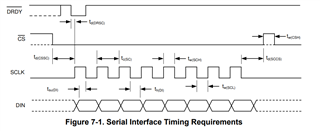
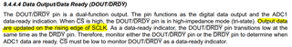
I've a question about the SPI timing of the ADS1262 device. The datasheet of the ADC says (Pg 10) that the delay time td(CSSC) from CS falling edge and first SCLK rising edge shall be 50 ns. But the sampling SCLK edge is the falling edge. The SCLK period requirement is 125 ns minimum. Does anyone know if reducing the delay time from 50ns to 0 ns, but increasing the period used to 1 us would work too or would have some problems? What is the real reason of the 50 ns requirement?

Datasheet: https://www.ti.com/lit/ds/symlink/ads1262.pdf?HQS=dis-dk-null-digikeymode-dsf-pf-null-wwe&ts=1744268007906&ref_url=https%253A%252F%252Fwww.ti.com%252Fgeneral%252Fdocs%252Fsuppproductinfo.tsp%253FdistId%253D10%2526gotoUrl%253Dhttps%253A%252F%252Fwww.ti.com%252Flit%252Fgpn%252Fads1262

Regards

Tiziano

  • Hi Tiziano Pigliacelli,

    You need to meet all of the timing specifications in the datasheet (I copied the serial interface timing below). As long as there is >50ns between CS low and SCLK high, this spec is met. So there is no need to add a specific tCSSC delay if the SCLK period is sufficiently long such that SCLK goes high 50ns after CS drops low

    These times are required to ensure that the ADC is internally able to respond to the applied signals (CS in this case)

    -Bryan

  • Ok thank you very much for the answer.

    My doubt is a little bit different: the ADC samples the data in falling edge of SCLK. If I use a slower clock, for example with period 1 or 2 microseconds, but I insert 0 ns of time delay between CS and rising edge of SCLK, do you think that it can be some problem? I used this way for years, and I've never had problems. So, my question is: the 50 ns requirements is necessary only in case of maximum SPI speed? So the real important requirement is the time from CS to the falling edge of the clock? Otherwise, what is the "action" that ADC performs in rising edge of the SCLK? Why 50 ns are necessary, if the sampling edge is the falling one?

    Thank you for your time
    Tiziano

  • Hi Tiziano Pigliacelli,

    Are you starting the SCLK period before you bring CS low? Most SPI peripherals I am aware of bring CS low and then start sending SCLKs. In this case, an SCLK period of 1us would never be an issue because there would be at least 500ns between CS low and SCLK high. So I'm not really sure what you are doing to cause this issue

    Also, yes, you must follow the datasheet timing requirements or it is possibly to cause issues with the communication. You violate these timing constraints at your own risk

    See below for why the ADC requires timing on both SCLK edges

    -Bryan

  • Hi Bryan,

    Thanks for your reply.

    I will try to explain my situation better.

    I have never had any operational problems, my goal is to understand why I have never had any problems using the device differently than what is stated in the datasheet.

    My usage only affects the input phase of the ADC (when I send commands), because the output phase meets all the timing requirements.

    When I send the command, the CS falling edge and the SCLK rising edge are simultaneous (not after, not before).

    The period is 1 µs, so the SCLK falling edge is 500 µs after the CS falling edge.

    The datasheet, in the input phase, states that the input data is sampled on the SCLK falling edge, so I understand that the device samples my request on the SCLK falling edge. This requirement is met in my case.

    The output phase meets all the timing requirements.

    In this specific case, I have seen the device work fine (for years).

    Maybe this is because the rising edge of the SCLK, in this input phase, is not really used, so the 50 ns requirement is not really important if the falling edge requirement of the SCLK is met? Is this interpretation possible?

    Sorry for the long answer, I hope I was clearer

    Tiziano

  • Hi Tiziano Pigliacelli,

    There is margin in many of our specifications to account for things like temperature and process variation. So it is possible that the device still communicated properly under the current conditions despite the fact that you are violating the timing requirements. However, you may encounter a set of conditions in the future that causes the the communication to fail. For example, process variation, which is not within your control

    Therefore, our recommendation is to meet the timing requirements provided in the datasheet by adding a short delay between CS low and SCLK high

    Again, if you choose to violate the timing (or any other datasheet) requirements you do so at your own risk

    -Bryan