This thread has been locked.

If you have a related question, please click the "Ask a related question" button in the top right corner. The newly created question will be automatically linked to this question.

ADS1251: CLK and SCLK input voltage range

Part Number: ADS1251
Other Parts Discussed in Thread: ADS127L11

Tool/software:

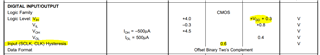
The datasheet states that the nominal CLK and SCLK input voltage is 0.6V, but doesn't specify a min or max allowable.  If I had a microcontroller deviate from normal configuration and apply VCC/logic high to the clock pin instead of an ~0.6V amplitude clock signal, will this cause damage to either of the CLK or SCLK pins?

  • Hi Elias Tarver,

    Any reason you are looking at the ADS1251 (from 2001) instead of a newer ADC? For example, the ADS127L11 released a few years back and is a better ADC in every possible performance and feature metric compared to ADS1251, at a similar price point. Or, if you can share more about what you are trying to measure, perhaps there is a more integrated device we can offer you.

    If you end up deciding to use the ADS1251 of course we can answer your question, I just want to make sure you are aware of all options

    -Bryan

  • Hello,

    I have no control over the design, so I cannot alter it with different parts.  I am simply trying to debug an existing PWA and gage what all may be a potential issue with it and/or damage caused by said issue.  

    I would prefer that my question got answered. 

  • Hi Elias Tarver,

    Understood.

    The only 0.6V spec related to the SCLK/CLK that I could find in the ADS1251 datasheet is with respect to the hysteresis. See the image below. Is this what you are referring to?

    Note that the maximum applied voltage on these pins is given by V_IH, which can be up to the supply (VDD). Also it should be noted that the max V_IL is 0.8V, so applying a 0.6V amplitude clock signal would just look like a constant 0 to the ADC

    -Bryan