This thread has been locked.

If you have a related question, please click the "Ask a related question" button in the top right corner. The newly created question will be automatically linked to this question.

ADS1261

Part Number: ADS1261

Tool/software:

Hi,

I am trying to measure 4 load cell's data (4 differential outputs; unipolar supply) at 400 SPS with gain 64 for a force platform. I have designed a breakout board for ADS1261 to connect all the load cells to it, amplify the raw data, and do the A/D conversion.

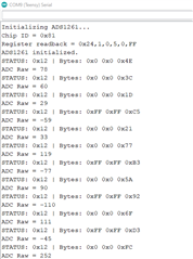
In the Schematic (the attached file), you can see that I have hard-wired the START, RESET, PWDN pins to DVDD and the CS pin to GND to keep the ADC always powered on, active and selected for serial communication. Now I am trying to establish the SPI communication between ADS1261 and Teensy 4.1 MCU. Teensy has a default SPI bus comprising pin 11(MOSI), 12(MISO), 13(SCLK) and 10(CS). Teensy's pin 11 (MOSI) is connected to the DIN pin of ADS, pin 12 (MISO) to the DOUT of ADS, pin 13 (SCLK) to the SCLK of ADS, pin 10 (CS) to the GND and pin 2 (GPIO) to the DRDY of ADS. I have defined all the necessary register assignment and Commands for conversion (you could check the attached code text; it is for one channel) still the ADS is not responding and MCU is reading some garbage values. Note: only one ADS is connected on the SPI bus, the bus is not shared among multiple slave devices. No internal reference is set, AVDD is set as reference. ADS chip id is getting identified as 0x81.

I am unable to understand where I have done wrong. It would be great if you could help me to resolve the issue.

With regards,

Charles

Code:

#include <SPI.h>

// Teensy 4.1 SPI0 default pins
#define DRDY_PIN 2

SPISettings spiSettings(1000000, MSBFIRST, SPI_MODE1);
#define INTER_COMMAND_DELAY_US 50

// Enable this to debug raw data and status
#define DEBUG_RAW_BYTES true

void safeDelay() {
  delayMicroseconds(INTER_COMMAND_DELAY_US);
}

void writeRegister(uint8_t reg, uint8_t val) {
  safeDelay();
  SPI.beginTransaction(spiSettings);
  SPI.transfer(0x40 | reg);  // WREG command
  SPI.transfer(0x00);        // Write 1 register
  SPI.transfer(val);
  SPI.endTransaction();
}

uint8_t readRegister(uint8_t reg) {
  safeDelay();
  SPI.beginTransaction(spiSettings);
  SPI.transfer(0x20 | reg);  // RREG command
  SPI.transfer(0x00);        // Read 1 register
  uint8_t val = SPI.transfer(0xFF);
  SPI.endTransaction();
  return val;
}

bool waitForDRDY(unsigned long timeout_ms = 1000) {
  unsigned long start = millis();
  while (digitalRead(DRDY_PIN) == HIGH) {
    if ((millis() - start) > timeout_ms) return false;
    delayMicroseconds(10);
  }
  return true;
}

int32_t readADCData(bool &statusOK) {
  uint8_t status;
  uint8_t data[4];

  safeDelay();
  SPI.beginTransaction(spiSettings);
  SPI.transfer(0x12);  // RDATA command

  status = SPI.transfer(0xFF);  // Read status byte
  for (int i = 0; i < 4; ++i) {
    data[i] = SPI.transfer(0xFF);
  }

  SPI.endTransaction();

  // Debug print
  if (DEBUG_RAW_BYTES) {
    Serial.print("STATUS: 0x"); Serial.print(status, HEX);
    Serial.print(" | Bytes: ");
    for (int i = 0; i < 4; i++) {
      Serial.print("0x"); Serial.print(data[i], HEX); Serial.print(" ");
    }
    Serial.println();
  }

  statusOK = !(status & 0x80);  // Bit 7 = 1 indicates ADC error

  // Combine bytes
  int32_t val = ((int32_t)data[0] << 24) |
                ((int32_t)data[1] << 16) |
                ((int32_t)data[2] << 8) |
                ((int32_t)data[3]);

  return val;
}

void setupADS1261() {
  delay(100);  // Wait for power-up
  SPI.beginTransaction(spiSettings);
  SPI.transfer(0x06);  // RESET command
  SPI.endTransaction();
  delay(10);
  writeRegister(0x01, 0x02);  // POWER: Internal reference off
  delay(10);
  writeRegister(0x02, 0x28);  // MODE0: SINC3, 400 SPS
  writeRegister(0x03, 0x00);  // MODE1: Single-shot mode
  writeRegister(0x04, 0x70);  // MODE2: 4-byte + SPITIM ON + STATUS ON
  delay(10);
  uint8_t mode2 = readRegister(0x04);
  Serial.print("MODE2 register readback = 0x");
  Serial.println(mode2, HEX); 
  writeRegister(0x10, 0x06);  // GAIN1: Gain = 64
  writeRegister(0x11, 0x23);  // INPMUX: AIN2 - AIN3

  delay(50);  // Let it settle
}

void triggerSingleConversion() {
  safeDelay();
  SPI.beginTransaction(spiSettings);
  SPI.transfer(0x08);  // START command
  SPI.endTransaction();
}

void setup() {
  Serial.begin(115200);
  delay(100);

  pinMode(DRDY_PIN, INPUT);
  SPI.begin();

  Serial.println("Initializing ADS1261...");

  // Read ID
  uint8_t id = readRegister(0x00);
  Serial.print("Chip ID = 0x"); Serial.println(id, HEX);
  if (id != 0x80 && id != 0x81) {
    Serial.println("Invalid ID. Check SPI wiring.");
    while (1);
  }

  setupADS1261();
  Serial.println("ADS1261 initialized.");
}


void loop() {
  triggerSingleConversion();

  if (!waitForDRDY(1000)) {
    Serial.println("DRDY timeout");
    delay(500);
    return;
  }

  bool statusOK = false;
  int32_t adc_raw = readADCData(statusOK);

  if (statusOK) {

    Serial.print("ADC Raw = ");
    Serial.println(adc_raw);
  } else {
    Serial.println("ADC Status Error Detected!");

  }

  delay(500);
}

  • Hi Charles Jebaraj,

    Can you please provide logic analyzer data showing the communication between the ADC and your controller? Please include CS, DIN, DOUT, SCLK, and the DRDY signal.

    This will allow us to see what you are sending to the ADC and how the ADC responds, as well as check timing (which is not evident from your code)

    -Bryan

  • Dear Bryan,

    For ADS1261- START, RESET, PWDN pins are hard-wired to DVDD, and CS pin is hard-wired to GND in PCB itself................For SPI communication between ADS1261 and Teensy 4.1 MCU, the default SPI bus0 is used- MCU's pin 11 (MOSI) is connected to the DIN pin of ADS, pin 12 (MISO) to the DOUT of ADS, pin 13 (SCLK) to the SCLK of ADS, pin 10 (CS) to the GND and pin 2 (GPIO) to the DRDY of ADS................. We don't have logic analyzer, so can't provide you the digital signals of the DIN, DOUT, DRDY and SCLK pins...... I have attached the modified code file here along with the output that we can see on the Serial port...... It is evident that the ADC chip id is correctly identified, the default register values are also read correctly, however the write register commands are all failing that's why probably the ADC read and conversion are not happening. Please help us to make it work....... Note: In our current hardware setup The ADS is always selected on SPI bus (as CS pin is tied permanently to low), and in continuous conversion mode (as START pin is permanently tied to DVDD); only one ADC is on the SPI bus....... In this setup how can we correctly establish the SPI communication and make the ADC work.....

    #include <SPI.h>
    
    // Teensy default SPI: Pin 11-MOSI, 12-MISO, 13-SCLK, 10-CS (GND)
    #define DRDY_PIN 2
    
    SPISettings spiSettings(500000, MSBFIRST, SPI_MODE1);
    #define INTER_COMMAND_DELAY_US 100
    #define DEBUG_RAW_BYTES true
    
    void safeDelay() {
      delayMicroseconds(INTER_COMMAND_DELAY_US);
    }
    
    void writeRegister(uint8_t reg, uint8_t val) {
      safeDelay();
      SPI.transfer(0x40 | reg);  
      SPI.transfer(0x00);        
      SPI.transfer(val);
    }
    
    uint8_t readRegister(uint8_t reg) {
      safeDelay();
      SPI.transfer(0x20 | reg); 
      SPI.transfer(0x00);        
      return SPI.transfer(0xFF);
    }
    
    bool waitForDRDY(unsigned long timeout_ms = 1000) {
      unsigned long start = millis();
      while (digitalRead(DRDY_PIN) == HIGH) {
        if ((millis() - start) > timeout_ms) return false;
        delayMicroseconds(10);
      }
      return true;
    }
    
    int32_t readADCData(bool &statusOK) {
      uint8_t status;
      uint8_t data[3];
    
      safeDelay();
      SPI.transfer(0x12);  // RDATA command
      status = SPI.transfer(0xFF);
      for (int i = 0; i < 3; i++) data[i] = SPI.transfer(0xFF);
    
      if (DEBUG_RAW_BYTES) {
        Serial.print("STATUS: 0x"); Serial.print(status, HEX);
        Serial.print(" | Bytes: ");
        for (int i = 0; i < 3; i++) {
          Serial.print("0x"); Serial.print(data[i], HEX); Serial.print(" ");
        }
        Serial.println();
      }
    
      statusOK = !(status & 0x80);  // Bit 7 = ADC error
    
      int32_t val = ((int32_t)data[0] << 16) |
                    ((int32_t)data[1] << 8)  |
                    ((int32_t)data[2]);
      if (val & 0x800000) val |= 0xFF000000;  // Sign-extend 24-bit to 32-bit
    
      return val;
    }
    
    void setupADS1261() {
      delay(100);  
    
     //writeRegister(0x01, 0x04);	// No reset, DRDY- Conversion data new
      writeRegister(0x02, 0x42);  // MODE0: SINC3 filter, 400 SPS
      writeRegister(0x03, 0x01);  // MODE1: Continuous conversion
      writeRegister(0x05, 0xD0);  // MODE3: SPITIM=1 (auto-reset), STATENB=1 (status on), Software PWDN
      writeRegister(0x06, 0x0B);  // REF: AIN0 - AIN1 (external 5V)
      writeRegister(0x10, 0x06);  // GAIN: 64
      writeRegister(0x11, 0x34);  // INPMUX: AIN2 - AIN3
    
      delay(10);
    
    
      Serial.print("Register readback = 0x");
      Serial.print(readRegister(0x02), HEX); Serial.print(",");
      Serial.print(readRegister(0x03), HEX); Serial.print(",");
      Serial.print(readRegister(0x05), HEX); Serial.print(",");
      Serial.print(readRegister(0x06), HEX); Serial.print(",");
      Serial.print(readRegister(0x10), HEX); Serial.print(",");
      Serial.println(readRegister(0x11), HEX);
    }
    
    void setup() {
      Serial.begin(115200);
      delay(100);
    
      pinMode(DRDY_PIN, INPUT);
      SPI.begin();
      SPI.beginTransaction(spiSettings);  // As CS is tied to GND
    
      Serial.println("Initializing ADS1261...");
    
      
      SPI.transfer(0x20); SPI.transfer(0x00);
      uint8_t id = SPI.transfer(0xFF);
      Serial.print("Chip ID = 0x"); Serial.println(id, HEX);
    
      if ((id & 0xF0) != 0x80) {
        Serial.println("Invalid ID. Check SPI wiring.");
        while (1);
      }
    
      setupADS1261();
      Serial.println("ADS1261 initialized.");
    }
    
    void loop() {
      if (!waitForDRDY(1000)) {
        Serial.println("DRDY timeout");
        delay(500);
        return;
      }
    
      bool statusOK = false;
      int32_t adc_raw = readADCData(statusOK);
    
      if (statusOK) {
        Serial.print("ADC Raw = ");
        Serial.println(adc_raw);
      } else {
        Serial.println("ADC Status Error Detected!");
      }
    
      delay(500);
    }

    With regards, 

    Charles

  • Hi Charles Jebaraj,

    I am not sure how to help without being able to see the communication. It is possible your code is correct but the communication timing is off. You will not be able to determine this just by reviewing the code.

    You will need some way to monitor the communication to at least check the timing requirements are met. But this will also help diagnose communication issues in general

    Also, I would not recommend holding CS low. Any glitch on the SCLK pin could either be interpreted as an additional SCLK period or a missed SCLK period, throwing off the entire communication. Yes it is possible to tie CS to ground, but again, not recommended because you must be very careful with the communication

    -Bryan

  • Thank you, Bryan