This thread has been locked.

If you have a related question, please click the "Ask a related question" button in the top right corner. The newly created question will be automatically linked to this question.

ADS7066: Daisy Chain Communication Issue with ADS7066IYBHT

Guru 12065 points
Part Number: ADS7066

Tool/software:

Hi,

We are currently using five ADS7066IYBHT devices in a daisy chain configuration:
FPGA → ADC0 → ADC1 → ADC2 → ADC3 → ADC4 → FPGA

We are trying to write 0x80 or 0x8A to the GENERAL_CFG register (Address: 0x01) of each ADC to enable the internal reference and perform offset calibration.

The protocol used is SPI-00 (default), and the SCLK frequency is 1 MHz.

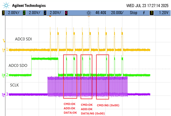
After sending the data 0x080180 (24-bit) from the FPGA to ADC0, the SDO output from ADC0 seems to show proper command/address/data timing. However, for ADC2, ADC3, and ADC4, the timing of the data output on SDO becomes misaligned, and the GENERAL_CFG register write does not succeed (the received command and data are 0x00).

We have attached oscilloscope waveforms showing this issue.

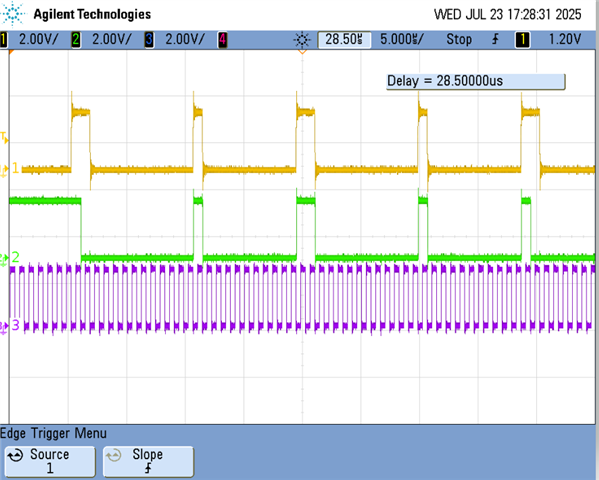
We would like to confirm the following points:

① Regarding the SPI-00 protocol timing
Is it correct that in SPI-00 mode, the ADC latches SDI data on the rising edge of SCLK and updates the SDO data on the falling edge of SCLK?

② Regarding the register initialization
We are currently setting the following registers during ADC initialization:

  • GENERAL_CFG register (0x01) = 0x8A
    → GENERAL_CFG[1]: CAL = 1 (ADC offset calibration enabled)
    → Is it required to perform offset calibration as part of ADC initialization?

  • OPMODE_CFG register (0x04) = 0x08
    → OPMODE_CFG[3:0]: CLK_DIV = 1000b (Sampling frequency = 62.5 kSPS)

If other registers must be configured to operate the ADC correctly in daisy chain mode, please let us know.

③ Hypothesis regarding the communication issue

We suspect that the issue may be caused by insufficient number of SCLK clocks when sending data to all 5 ADCs.

Since the chain consists of 5 devices, we believe that 24 bits × 5 = 120 bits of SCLK are required in a single SPI transmission to propagate data correctly through all devices.

However, we are currently sending 24-bit command/address/data (0x080180) sequentially 5 times, which may not be enough to allow the downstream ADCs to receive and pass on data via SDO.

④ Questions to confirm

  • Is it necessary to send 120 SCLK clocks in a single transmission when writing to 5 ADCs in daisy chain mode?

  • Alternatively, is it valid to send 5 sets of 24-bit commands separately, as long as additional SCLK clocks (24 × (N−1) = 96 bits) are sent after to allow data propagation through the chain?

  • Are there any other timing or configuration points that we should be aware of when operating ADS7066 in daisy chain mode?

We appreciate your confirmation and support.
Oscilloscope captures and circuit schematics are available upon request. Please let us know if you need further details.

Best regards,
Conor

  • Hello Conor, 

    Thank you for your question and the thorough explanation!

    • Yes, with SPI-00 latches on the rising edge and transitions on the falling edge. 

    • General CFG looks good! Offset calibration is not required, but it is recommended. OPMODE_CFG looks good too if enabling the CLK_DIV is the goal
      1. Here I wanted to note that the oscillator divided (CLK_DIV) should only be used when Averaging is enabled.
        1. When averaging is enabled a single conversion is needed and all the subsequent conversions are generated internally, the rate of this internal conversion is set by the registers in OPMODE_CFG.
        2. Otherwise, the conversion rate should be determined by the CONVST pin signal. If a sample rate of 62.5ksps is needed without the averaging mode then the SPI/SCLK would need to be adjusted accordingly.
      2. Do you plan to enable the averaging module?  
      3. Could you try writing to the device without setting a value on OPMODE_CFG/CLK_DIV?
      4. Daisy chain does not require register configurations, maintaining the CS low, providing sufficient SCLKs, and connecting the devices following Figure 7-7 in the datasheet is all that is required. 

    • 120 SCLKs should be enough for 5 devices. 
      1. When the device continues to receive SCLKs while the CS remains low in goes into daisy chain mode and outputs what came in through SDI through SDO.
      2. So in your case with 5x devices, the 1st 24 SCLKs will write to device 0, maintaining CS low, the input will not be seen on SDO0 until the next 24 SCLKs like we see in the image you shared. Meaning that device 1 will have the command sent during the 25-48 SCLKs, device 2 during 49-72 SCLKs, device 3 73-96, and finally device 4 with 97-120.
      3. If you would like to readback the value in your FPGA then an additional 24 SCLKs would be needed. 
      4. Is there a particularly long distance between the 5 devices as well as the FPGA?
        1. At 1MHz I wouldn't be too concerned unless they are very far from each other
        2. If comparing the SCLK input of the 1st and last device (or closest and furthest devices), is there a substantial delta?

    • A single N x 24 SCLKs are not required, burst mode would work fine, as long as the total is still the Nx24 (120 for 5 devices)

    • An important timing to consider when using daisy chain is the data throughput rate (1/t_cycle)
      • The devices simultaneously receive the command to start conversion which should not take longer than 3.2us, followed the Nx24 SCLKs, and finally a t_quiet before CS can be brought high again.
      • when in daisy chain it can be said that t_cycle = t_conv + N*(24*t_SCLK) + t_quiet 
        • For the 62.5ksps, t_cycle = 16us 
        • t_SCLK = (t_cycle - t_conv - t_quiet)/(N*24) --> (16us - 3.2us - 20ns)/120 = 106.9ns --> SCLK = 9.4MHz
        • With SCLK = 1MHz
          • t_cycle = 3.2us + (120*1us) + 20ns = 123.22us --> sample rate = 8.1ksps 
    • Aside the throughput it would be important to make sure that the set up and hold time if SDI are met (t_su_ckdi & t_ht_ckdi respectively), again with 1MHz I wouldn't think this would be an issue, but making sure would be good.  The bigger concern would be if the devices were far apart and the SDI/SDO signal degraded, or if they are far apart and with a buffer if the buffer added some delay or something similar to this. 
      • From your image I can see that some bits were lost as well as the yellow signal also appears to be more degraded than the green, it is difficult to confirm with the images shared but if you could confirm if the SCLK rising edges are aligning with the expected SDI signal, and if not, if they correlate with what is seen on SDO

    Best regards, 

    Yolanda 

  • Hi Yolanda,

    Thank you for your reply.

    ① Regarding the Conversion Cycle and Sampling Rate
    For example, if the desired sampling rate is 62.5 ksps, the target conversion cycle (t_cycle) should be approximately 16 µs.

    To meet this requirement, the necessary SCLK clock period can be calculated as:
    (16 µs − 3.2 µs − 20 ns) ÷ 120 ≈ 106.9 ns,
    which corresponds to an SCLK frequency of approximately 9.4 MHz.

    Since we aim to operate at a sampling rate of 62.5 ksps, is it correct to understand that the minimum required SCLK frequency is approximately 9.4 MHz?

    The conversion cycle (t_cycle) can be calculated using the following formula:
    t_cycle = t_conv + N × (24 × t_SCLK) + t_quiet

    Therefore, reducing t_SCLK (i.e., increasing the SCLK frequency) shortens the t_cycle, making it possible to operate at sampling rates higher than 62.5 ksps.

    Based on this, we believe that an SCLK frequency of at least approximately 9.4 MHz is necessary to achieve 62.5 ksps operation.

    ② Regarding OPMODE_CFG and SCLK Frequency

    • We have configured OPMODE_CFG = 0x08 (i.e., CLK_DIV = 8).

    • According to the datasheet, the CLK_DIV setting is used only when the Averaging mode is enabled.

    • Therefore, if the Averaging function is not used, it is recommended to omit the OPMODE_CFG setting and verify operation accordingly.
      (Reference: ADS7066 Datasheet – Page 18)

    Based on our review of the ADC datasheet, it appears that the sampling rate and conversion cycle (t_cycle) can be modified via the OPMODE_CFG register.

    As you explained, the SCLK frequency must be properly configured to match the selected sampling rate and conversion cycle (t_cycle).

    When using the default configuration for OPMODE_CFG (OSC_SEL = 0, CLK_DIV[3:0] = 0100),
    the sampling rate is 250 ksps and the conversion cycle (t_cycle) is 4 µs.

    In this case, the required SCLK period is:
    (4 µs − 3.2 µs − 20 ns) ÷ 120 ≈ 6.5 ns,
    which corresponds to an SCLK frequency of approximately 153.4 MHz.
    Is this understanding correct?

    To reduce the required SCLK frequency, we have configured CLK_DIV[3:0] = 1000 in OPMODE_CFG.

    Although the Averaging mode can be enabled or disabled through the OSR_CFG register,
    we do not intend to use the Averaging function in our application.

    ③ Regarding Daisy Chain Communication and ADC Initialization

    Thank you very much for your detailed explanation regarding Daisy Chain communication and the SCLK transmission method.

    Currently, the FPGA generates the communication timing according to the specifications of Daisy Chain mode, so we believe there are no issues with the timing itself.

    However, we are observing waveform distortion, and there is a possibility that the ADC0 device may be damaged. We are currently proceeding with a component replacement.

    Just to confirm, we would appreciate your guidance on the following two points regarding ADC initialization:

    • Is it necessary to reset the ADC before configuring each register?
      We understand that the ADC can be reset by setting the RST bit in the GENERAL_CFG register to "1".
      Could you please confirm whether this step is required prior to register configuration?

    • The following URL points to a C-language sample code for controlling the ADS7066:
      https://github.com/TexasInstruments/precision-adc-examples/blob/main/devices/ads7066/ads7066.c
      In the sample code, there is an initADS7066(void) function that performs the ADC's initial configuration.
      Based on this function, it appears that we need to clear the BOR flag.

      According to the datasheet, the BOR bit in the SYSTEM_STATUS register can be cleared by writing "1" to the bit ("Write 1b to this bit to clear the flag").
      Could you please confirm whether it is necessary to clear the BOR bit during ADC initialization?

    We would appreciate your confirmation on these points.
    Thanks,

    Conor

  • Hello Conor,

    1. Correct, to configure the sample rate when in daisy chain what needs to be configured is the SCLK as you showed. 
    2. When averaging is not enabled, OPMODE_CFG configuration should be omitted. The default value is set to 100b because the is the highest limit for the ADS7066. It should only be set to 1000b or any other value if averaging is enabled.
      1. Ideally if 250ksps was the goal with 5 devices in daisy chain, yes, 153.5MHz would be required for the SCLK. However, the SCLK does have a max limit of 60MHz so this would not be possible.
      2. With 5 devices in daisy chain the maximum sample rate would be ~190ksps (if using SCLK = 60MHz and a controller that would allow for the other SPI timing requirements needed).  
      3. When in daisy chain and averaging is not enabled, please configure sample rate like the example you shared in part 1. 
    3. Could you please share more information on the type of distortion that is being seen? 
      1. Reset is not required for every single register write, in fact, resetting the device will return all registers to default values. 
      2. As for initialization, we do recommend a reset is done after initial power-up, followed by clearing the BOR flag in the SYSTEM_STATUS register, it is a good practice, but its not always required. 
        1. The BOR bit in the SYSTEM_STATUS register is an indicator of a flag that is set a power-cycle or reset event is detected. This register can be cleared by writing a 1 to it, which is recommended as well, but its not required. 
        2. Additionally we also recommend performing an offset calibration (setting CAL to 1 in GENERAL_CFG register) after power-up/reset, and periodically during extended operation to maintain optimal performance.

    I wanted to include some additional information to explain why any configuration of OPMODE_CFG should be omitted if averaging is not enabled. 

    The ADS7066 operates in One-Shot Conversion mode, where a single conversion is triggered by the CS rising edge. When CS goes high, the device generates an internal convert-start signal to begin the conversion of the previously acquired sample. Unless averaging is enabled, the internal convert-start signal occurs once between CS rising edges, allowing the controller full control of the sample rate, limited only by timing constraints (t_cycle ≥4µs, enough time for t_conv and t_acq ≥800ns along other requirements set in the table 6.6 and 6.7 of the datasheet).

    For slower sample rates, simply increase the time between CS rising edges (e.g., slower SCLK, longer t_quiet). 

    When averaging is enabled (OSR_CFG), the device internally generates N conversions after a single CS rising edge, using an internal oscillator. Timing for this is set via OSC_SEL and CLK_DIV (see Table 7-3). The controller no longer drivers the sample rate, the internal timing takes over until averaging is complete. 

    If averaging is not enabled, omit any OPMODE_CFG configuration. 

    I hope this helps, in the use case explained with 5 devices in daisy chain and 62.5ksps, I would recommend following your example in section 1 and setting the SCLK to 9.4MHz as well as omitting any configuration on OPMODE_CFG.

    Is 9.4MHz an option in your current system? or is 62.5ksps a hard requirement? 

    Best regards, 

    Yolanda