Tool/software:
Hello, I am an AFE chip user of Chinese medlander,we are currently encountering some questions, and I hope to get answers from you.
The ADC model is AFE58JD28, the sampling rate is 40M, each LANE corresponds to 8 ADC conversions, the JESD204B configuration rate is 6.4GBPS, F is equal to 16, K is equal to 2, the reference clock is 200M, the DRP clock is 160M, and the current PLL type is CPLL.
The configuration for AFE initialization is:
010074,021000,038019,040001,180F00,240F00,300F00,3C0F00,C54000,C60000,C900C0,CA0000,CE0006,D00001,DD0000,DE00C3,DF0040,4A1C00,4B0120,4D00F0,500002,554020,730010,911754,9A0400,9B2772,418000,428000,410000
The configuration of Profile RAM is as follows:
00990000 00000480 00008003 00FFFC00 00000020
00990000 00000480 00008003 00FFFC00 00000020
00990000 00000480 00008003 00FFFC00 00000020
00990000 00000480 00008003 00FFFC00 00000020
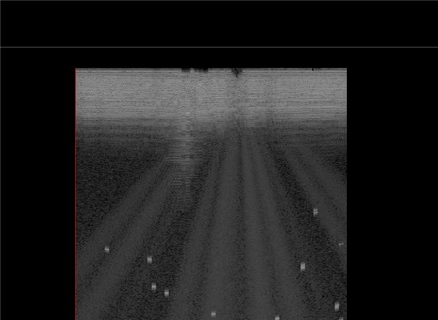
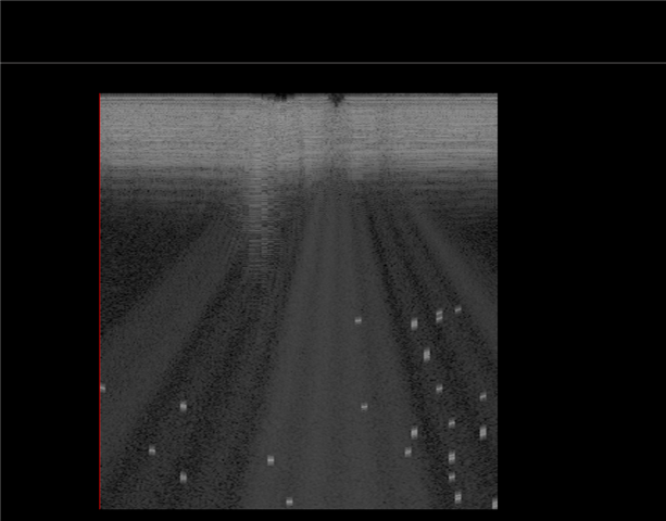
The image has this figure-eight fan-shaped area.
Excuse me:
(1) What are the reasons for this? How should I test and troubleshoot?
(2) How can AFE and JESD204B be tested separately for data transmission problems?
(3) There are currently only two lanes on the hardware, if the rate is reduced by 3.2G, will the imaging quality be affected under the premise that the sampling rate remains unchanged?
(4) If there is a problem with the decoding of the JESD channel, but the problem channel is relatively random, how to determine the problem and how to solve it?
The following images are currently found during imaging