ADS8598S: Inquiry regarding right selection and features of ADS8598S ADC

Part Number: ADS8598S
Other Parts Discussed in Thread: ADS9813, ADS8688W

Tool/software:

Hi Team,

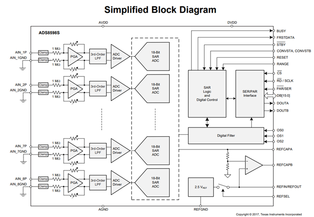
We are planning to use the ADS8598S ADC in the data acquisition system, and want to make sure to fulfill this requirement:

- The input voltage range for each channel has an upper bound of ± 50 V (100 VPP) and a lower bound of <= ± 1 V ( 2 VPP).

 Could you please let us know how this requirement can be fulfilled to support both the upper and lower limits of the voltage?
During our quick exploration, we found the PGA281 chipset. Maybe this can be useful for our requirement. Please confirm.

Let us know if this is the correct way to satisfy the above-mentioned requirement. Also, let us know if you have a better, cost-effective solution.

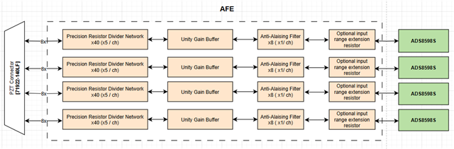
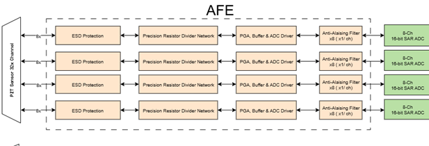
Attached is the basic architecture diagram for a more detailed understanding.

Thanks & Regards,
Sahil Nayak

  • Hello Sahil, 

    I am not able to see the 1st image shared, did it have relevant information aside the line below? 

    - The input voltage range for each channel has an upper bound of ± 50 V (100 VPP) and a lower bound of <= ± 1 V ( 2 VPP).

    In your 2nd image, with the AFE block diagram, is the ±50 V the input of the "Precision Resistor Divide Network" block? What would be the expected output range after that block? 

    The ADS8598S has an integrated PGA, LPF, and ADC driver with an input range of up to ±10V. If the output of the "Precision Resistor Divide Network" block is within that range then the ADS8598S would be able to replace half of the AFE block.  

    The ADS8598S also has a constant input impedance that can be leveraged to further increase the input range beyond the ±10V, below is a table of the performance up to ±40V. Please see the Typical Applications section of the datasheet for more information as well as these reports: 

    Circuit To Increase Input Range on an Integrated Analog Front End (AFE) SAR ADC

    Extending Input Voltage Range and Understanding Associated Errors for ADC With Integrated Front End

    Reducing effects of external RC filter circuit on gain and drift error for integrated analog front ends (AFEs): ±10V


    Best regards, 

    Yolanda

  • Hi Yolanda,

    Thank you for the details.

    Please see the attached table below:

    Vpp (+/-) R1 (kohm) R2 (kohm) Vo
    50 400 100 10
    40 400 100 8
    30 400 100 6
    25 400 100 5
    20 400 100 4
    10 400 100 2
    5 400 100 1
    2 400 100 0.4
    1 400 100 0.2

    Vpp is the input voltage from the sensor.

    R1 and R2 are the precision voltage divider network

    Vo is the voltage to the input of the ADC.

    We believe that, as per the table, ADS8598S will be able to accept all the values of Vo listed in the table. However, we are looking for clarity of operation for the last 2 rows of the table, where the input voltage to the ADC will be 400mV and 200mV.

    Since the ENOB for ADS8598S is 15.3 bits, the minimum voltage that ADS8598S can read will be 61.96uV. So, as per these calculations, it will be able to read 200mV and 400mV input voltage too with precision.

    Please confirm our understanding and correct me if I am wrong.

    Thanks & Regards,
    Sahil Nayak

  • Hello Sahil, 

    Correct, the ADS8598S will be able to measure the 0.4V and 0.2V ranges with precision. I would still recommend some additional system calibration to be done for better performance. 

    Best regards, 

    Yolanda

  • Hi Yolanda,

    Thank you for your confirmation.

    I have updated the interfacing block diagram as per the discussion, as shown below:

    Please let us know if any additional system calibration needs to be done for better performance.
    If yes, kindly provide the reference for the same.

    Thanks & Regards,
    Sahil Nayak

  • Hello Sahil, 

    The additional calibration could be done with known system inputs, if a couple fixed values near the end ranges of the ADC can be set then that is all that is needed.  This would be more important if the optional range extension resistor is added, but it is good practice either way. 

    Aside that, the block diagram looks good. 

    Best regards. 

  • Hi Yolanda,

    Noted. Thank you for the information.

    The last thing I would like to confirm is whether the calibration we do will be applicable for the temperature as well?

  • Hi Yolanda,

    Do you have any updates to share on this?

  • Hello Sahil, 

    Apologies for the delay, I was on holiday. 

    The calibration will certainty help over temperature as well, as shown in the Reducing effects of external RC filter circuit on gain and drift error for integrated analog front ends (AFEs): ±10V

    Best regards, 

    Yolanda

  • Hi Yolanda,

    Thanks for the update.

    If I want to do the calibration with respect to the temperature, then which parameter from the datasheet should be my base reference and how should it be used in the calibration? Gain error temperature drift?

  • Hello Sahil, 

    Correct, gain error drift, offset error drift , and if using the internal reference, internal reference and reference buffer drift  would be great indicators of the expected over temperature drift. Depending on the full signal chain the other components in the system exposed to the temperature should also be considered. 

    Do you expect temperature flocculation for the system or is it likely to remain at somewhat consistent temperatures once the system is stabilized?  

    If it will remain within a consistent temperature after stabilization, I would suggest recalibrating at that temperature and the drift values would not be required. 

    If it is expected to fluctuate, then yes, considering the drift performance of the ADC as well as any components in the signal path would be a great place to start. Or a system drift calibration can be done where the system calibrates and a typical and ~min/max expected temperatures and a calibration look-up table can be done, this is also encouraged if multiple parameters would be changed, 

    Best regards, 

    Yolanda 

  • Hi Yolanda,

    Thank you for the information.

    I have one more question to ask, which is related to the selected ADC ADS8598S.

    We have one requirement of "digitally-adjustable input ranges". Will the selected ADC suffice this requirement?

    If not, do you have any other ADC part suggestion that can suffice this requirement?

  • Hello Sahil, 

    We have a few options for ADCs with digitally-adjustable input ranges

    If you need all channels to be simultaneously sampled we have the

    •  ADS9813 - for simultaneous sampling with 18-bit, 2MSPS and input ranges of: ±12V, ±10V, ±7V, ±5V, ±3.5V, and ±2.5V
    • ADS9803 - the 20 bit version of the ADS9813 with 20-bit, 2MSPS, and the same input ranges 
    • ADS8598S and ADS8598H (previously selected) are also 18-bit but at a slower 200kSPS and 500kSPS respectively and with only ±10 V and ±5 V input ranges

    If simultaneous sampling is not required and a multiplexed input ADC is an option we have 

    • ADS8698 - 18-bit, 500kSPS with input ranges ±10.24 V, ±5.12 V, ±2.56 V
    • The 16 bit version of this device: ADS8688A : has input ranges of ±10.24 V, ±5.12 V, ±2.56 V, ±1.28 V, ±0.64 V
    • There is also a version of this device that is in the process of being released: ADS8688W that will have the same input ranges except the larger input range will be ±12.288V
      • the single channel version of this has already been released ADS8681W)

    What is the timeline of your design? 

    Best regards, 

    Yolanda

  • Hi Yolanda,

    Thank you for your suggestions. I will check it further.

    We are about the start the design in October.