Other Parts Discussed in Thread: , SN65LVDS100
Tool/software:
Hello
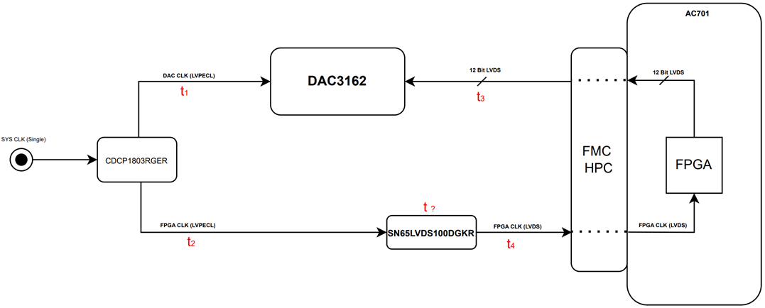
I'm designing a PCB board with an FMC interface, including a DAC3162. I'm using the DAC3162EVM and the FMC Adapter card as references in the design.
This board will connect to the AC701 FPGA board via the FMC connector.
It also includes an LVPECL to LVDS buffer (lvds100dgkr) integrated circuit to receive the LVPECL clock signal as lvds on the FPGA.
I'm not sure how to adjust the delay times when doing length matching on the PCB.
The datasheet states that the setup and hold times should be at least 200ps.
What should I consider to achieve this delay in the PCB design?
I've added a block diagram for better understanding. Currently, the delay values are approximately as follows:
T1 = T2 = 360ps
T4 < 10ps
T3 = 300ps
I believe the lines on the FPGA board have equivalent delays.
Also, how should I account for the internal delay of the SN65LVDS100 integrated circuit?
I need help determining the delay values for the clock line and data line.
Thank you.