ADS1675: Strange SPI data (samples shifted by one bit)

Part Number: ADS1675
Other Parts Discussed in Thread: TXU0101

Tool/software:

Hi
we have a custom board with the ADS1675 and we observe a strange issue: Sometimes two samples samples in the data stream is shifted. One sample is shifted left and the following is shifted right one bit. We are operating the ADS1675 with the following parameter:
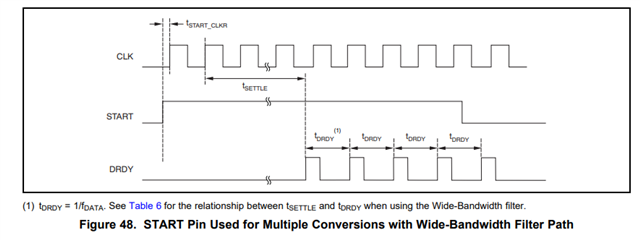
  • MCLK= 20 MHz
  • Output data rate 2.5 MHz
  • DRATE set to "101"
  • LL_CONFIG = high
  • FPATH = Low

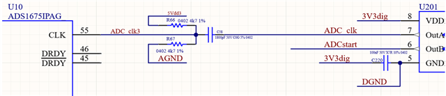
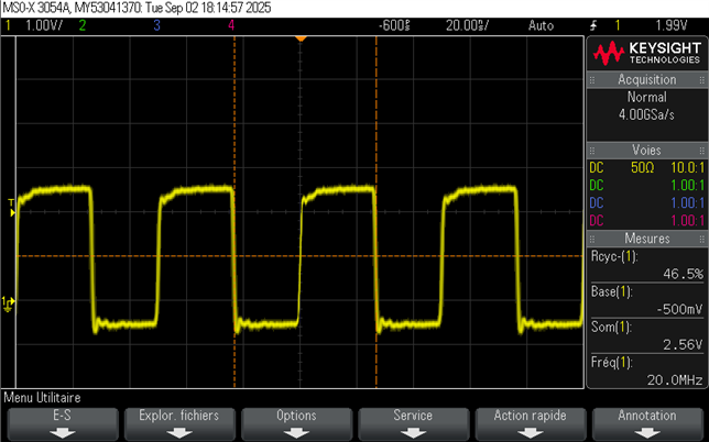
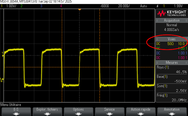
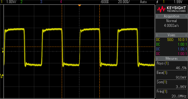
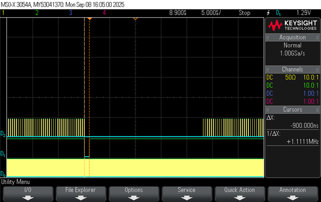
 We are reading the data using an FPGA and my first guess was that this must be a timing issue of the FPGA. After thorough investigation it turned out that the shifted data must be coming out of the ADC:


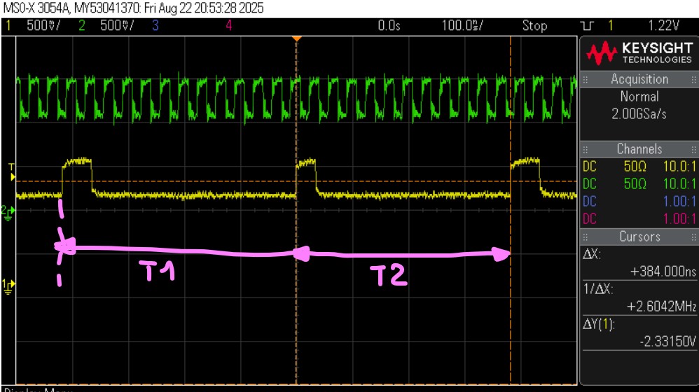
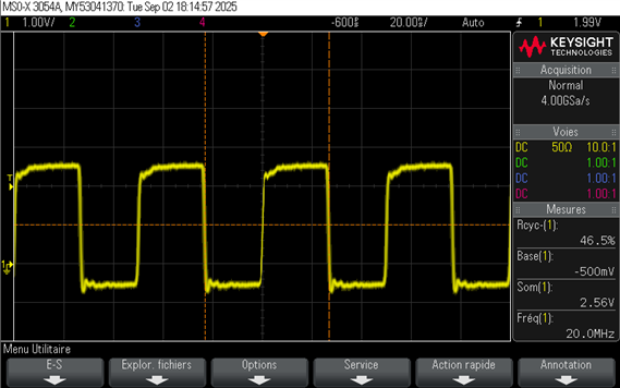
The green channel 2 is showing SCLK div 2 (Divided by a D-FF) and the yellow channel is the DRDY signal from the ADC. During normal operation the period between two DRDY pulses is 400 ns ( @ 2.5MHz ODR). The screenshot shows that there is a long period T1 = 416 ns with 25 clock edges followed by a short period of 384ns with 23 clock edges. This explains the two wrong samples, one shifted left, the other shifted right.

My question is now: What could cause the ADS16575 to behave like this ??? 

Kind regards
Reto

  • Hello Reto,

    Are you keeping the START pin high for multiple conversions, as shown in Figure 48?  If not, then the timing of DRDY will depend on the timing of the provided START signal.

    The ADS1675 clock circuit is part of the analog domain, which requires a 5V CMOS level clock input.  Please confirm that the clock input levels are correct.  If using 3V logic levels, you can get erratic operation due to not meeting the minimum 3.5V input high threshold for the clock input.

    I suggest using your scope to directly measure the clock signal on pin55 of the ADS1675 package.  If there is excessive ringing, this can also cause unexpected behavior.

    If the power supply bypass capacitors are not included or are not located directly next to the package pins, this can also cause signal integrity issues (Figure 52).  If you could include an image of the schematic showing the ADC connections, as well as an image of the ADC layout, I will review to see if there are any other concerns.

    Regards,
    Keith Nicholas
    Precision ADC Applications

  • Hi
    thank you for your quick reply and detailed reply! I have checked these points and it appears that we do have an issue with the clock input. In our design AVDD is 5.2V and the clock comes from a 3.3V logic supply. In order not to introduce additional clock jitter, we do the level translation with a dc decoupling circuit that pulls the dc level of the clock signal to AVDD/2.

    When we measure the clock at the input of the ADC we observe a dc shift of approx. -900 mV as soon as we apply the clock:


    We then suspected that the upper logic level (0.7*AVDD) could become critical due to that dc shift. We have then shifted the clock signal up and down by changing the resistor values of the pull-up and pull-down resistors that are defining the dc level.

    The surprising outcome of these tests is, that we see the issue (1 bit shifted samples) when we pull the dc-level up even though the logic levels with respect to 0.3/0.7VDD are looking better. In the other direction we can pull the dc level down and everything appears to work stable. Here is an example where the logic low level is -500mV and the high level is 2.56V which is completely out of specifications but it works perfectly:


    So to summarize: If the logic levels are within the 0.3/0.7AVDD specification we see the issue, if we are using lower levels it appears to work!

    Does this make any sense to you?

    Kind regards
    Reto

  • Hi Reto,

    I see channel 1 is configured for DC 50Ohm.  This is likely loading the clock signal and not providing an accurate measurement.  Set channel 1 to Hi-Z and then verify your measurements.

    If the clock signal is less than -0.3V, then this will cause the internal ESD diodes to conduct and could result in unexpected operation.

    Regards,
    Keith

  • Hello Keith

    I'm using an active differential high speed probe with 1MOhm/1pF input impedance and my scope sets the 50 Ohm automatically. I guess that 50 Ohm is the output impedance of my active probe. 


    It appears that I see the issue, as soon as the low level of the clock signal is > approx. 0.3V.


    With the following clock signal I clearly see the issue:

    According to my understanding these input levels are within the specification because:
    900mV < 0.3*AVDD
    4V > 0.7*AVDD

    So why is this setup not working?
    Can you confirm that the clock input specification of the ADS1675 (0.3 / 0.7AVDD) is correct?

    Best regards
    Reto

  • Hello Reto,

    O.K., understood you are using a differential probe.  Can you confirm that you are measuring the differential clock signal at the CLK and AGND pins of the ADS1675?

    Also, are you using a split ground plane for AGND and DGND, or a single solid ground plane?  I suspect that the ADS1675 device sees ringing on the CLK input with respect to AGND.  This could be caused by the ground topology on your board, or even power supply bypass capacitor placement.  If you could include an image of your board, or board layout around the ADS1675, I will take a closer look.

    The digital input cells are standard cells used on many TI products that have been tested over temperature, voltage, and process.  The CLK input should easily tolerate the datasheet spec for a typical part at room temperature.  Other than some type of signal integrity issue, I do not have a good explanation.

    Regards,
    Keith

  • Hello Keith
    yes we do have a splitted GND planes for AGND and DGND and yes the ADC CLK is generated in the DGND domain BUT all the above measurement  of the clock signal were made with respect to AGND! When I measure the CLK signal with respect to DGND it looks the same. I have also measured DGND with respect to AGND but I can't see significant noise. It's really confusing, because on one side I can replicate the issue by changing the low level of the clock signal, on the other side the clock signal looks o.k.

    Regarding your other idea that the issue could be related to the start signal timing. This is how the timing looks like:
      
    D0 CLK
    D1 Start
    D2 DRDY

    The start signal normally is high. To synchronize multiple ADS1675 we pull the start signal low for approx.1 us. Could that low pulse be too short?

    Best regards
    Reto 

  • Hello Reto,

    The minimum START high is 2 t-CLK, or 100ns using a 20MHz clock.  The minimum START low period will be similar, so I doubt this has anything to do with timing discrepancy.

    Based on your prior tests, this does seem to be related to the clock amplitude, although your clock levels are within specified requirements.  The only other explanation I have is power supply bypass capacitor placement and grounding.  You mentioned using split AGND and DGND planes.  If these are not connected together near the ADC package, then you could try providing a local short between these grounds at the ADC package to see if this makes a difference.

    I think adding a voltage level translator that drives the clock input close to ground and AVDD will solve your problem, but there is likely some other noise issue with the device on the layout that is making the clock input more sensitive to noise than expected.  We have used a voltage level translator gates with good results, such as TXU0101.

    Regards,
    Keith