This thread has been locked.

If you have a related question, please click the "Ask a related question" button in the top right corner. The newly created question will be automatically linked to this question.

Connecting ADS1294

Other Parts Discussed in Thread: ADS1294, ADS1298

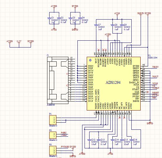
Hello everybody, This is my first post in this forum, I hope someone can give me some advices for my project.  I'm going to work with an ADS1294 in my university project and I have some doubts about the connections. At first I'm going to describe in brief my project, I have to design an ECG system, it has to be portable so I have constraints about the size of my PCB that's why I think about to use a basic connection of this device , I mean I want to use the minimum number of components and get the best performance as possible of my ECG system. My issue is that I'm not completely sure about my schematic, I'm using the connection that I saw in the datasheet (Connecting the Device to Unipolar (+3V/+1.8V) Supplies) but I don't know if this configuration is enough for getting a good performance of the ADS1294 besides I want to use a single 3.3v power supply in order to save space.

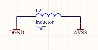
This is my configurations: Single 3.3v supply, Internal reference 2.4v, Internal oscillator that's why I connected the CLKSEL to DVDD, I won't use GPIO the dataha sheet says that I have to connect this pins to ground if they aren't used is this necessary?, I won't use the RLD pins in order to save space in the PCB  I know this are used to reduce noise do you think RLD is really necessary?.

This is my schematic for the ADS1294

you can ignore the HDMI port and P2 and P3 headers.

I would like to thank everyone who helped me, All advices are welcome. I'm sorry if I made mistakes in my English grammar I still have to improve it.

  • Hi Alxgro!

    Welcome to our forum and thank you for your interest in using the ADS1294 in your project.  We'll take a look over your schematic and give you feed back shortly.  Please feel free to 'search' this forum for ADS1298 and ADS1294 related posts, you may find some useful information.  There is also a 'Frequently Asked Questions' page here which you might find helpful:

    http://e2e.ti.com/support/data_converters/precision_data_converters/w/design_notes/frequently-asked-ads1298-and-ads1198-questions.aspx

  • Hello,

    thank you so much, I'll wait for the answer. I've been looking around the forum and I've find interesting information that may be useful for my project.

    Thanks again.

  • Hello again!!!

    Has anyone found something wrong in my design?, I want to do some tests, but I don't want to waste my ADS1294 in a design that could not work, That's why I'm looking for assistance. I hope someone can give me some advices.

    Thanks.

  • Hi Alxgro,

    Sorry for the delayed response here.  We've looked over what you posted and see no immediate issues with your schematic.  Implementing the RLD will help reduce noise though.  Since this is a very small board, you might be able to get away with good local shielding.  Send us your Gerber files once your layout is complete and we'll look over them for you as well.

  • Hello!!

    Thanks for your answer. technics of shielding, It would be great if you can give some advices about that. These are my gerber files, In the top layer I have the ADS1294 in the left side and my MCU in the right side and I have a 3.3v voltage regulator and a usb isolator in the bottom layer.

    by the way, I have another doubt with analogical and digital ground (AVSS and DGND), I have routed these tracks separated form each other and I use and inductor in order to get them together in one point on my PCB layout. I read about this technic on internet but I'm not completely sure if it's correct.

    I couldn't attach my gerber files, it said that This type of file is not allowed, can you give an e-mail address for sending my files?

    Thanks a lot for your help.

  • Hi alxgro,

    I've messaged you with my email address. Please forward your Gerber files, and we'll be happy to take a look at it :)

  • Hi alxgro,

    One of the most important pieces here is to realize the amplitude of interest in ECG systems is about 5-10mV. (for further clerification, you may go HERE - to the design notes page)

    The reason why this is so important to note, is because a sufficient return path from ground is dire, in these high precision cases. In our system, we have four layer boards, with one being the ground plane. Wire-to-wire grounding is not sufficient for signals this small. So, specifically, in your layout, I suggest adding an additional layer to be your ground plane, and refrain from the small ground traces. Filling the "dead copper" with grounding is also a good practice.

    What is your AVSS value? With AVDD=3.3V, I'm assuming that AVSS=gnd? [Typically, people have one of two configurations: 1)+/- 2.5V, OR 2) +3.3V and Gnd]

    If AVSS is gnd, then it would also be good practice to tie AVSS to the ground plane as close to the chip as possible. Same is true with DGND. With the important add-in that AVSS and DGND should be tied together, not separated.

    What is the SO8 component that you have?

    These are the main notes that I find, that could be an issue.

    As far as the input circuitry, it is VERY important to have input protection circuitry. We can not really give specifics, as they will depend on the standards your end equipment needs to meet. There are different regulatory requirements, based on the classification of an end product (medical has IEC 60601, for example), which has specific criteria for patient protection. 

    Hope this helps!

  • Thanks for your help,

    Exactly, my AVSS value is GND. So, should I remove the inductor that I'm using to tie together AVSS and DGND and use a simple wire?, it doesn't appear in the schematic above but I have something like this:

    The SOIC8 is a 3.3v regulator (MCP1727) I'm taking 5v from USB and I use the MCP1727 to get the 3.3v in order to supply the ADS1294 and my MCU.

    As far as the input circuitry, I'm going to make a special cable for my electrodes I think I'm going to implement the protection circuitry within the cable. I didn't take in count this but I was checking out this document (http://www.ti.com/lit/ug/sbau171a/sbau171a.pdf) and I realized that there was a stage with some circuitry before the inputs. Thanks for the advice.

    I'm going to implement what you told me, can I send you my gerber files again after I do all the modification to my PCB layout?

    I appreciate all your help.

  • alxgro,

    Well, I suppose there's nothing technically wrong with tying them together with an inductor. But, perhaps the best way would be to just remove the inductor, and short them to the same ground plane. If anything, that's one less component you have to worry about :).

    Certainly! I would not mind looking over the changed gerbers.

  • can i use ADS1294 for EMG signals?? What will be the circuit for that kindly help