hello,everyone,
I am trying to do some evaluation on ads62p29 EVM_rev_C board.
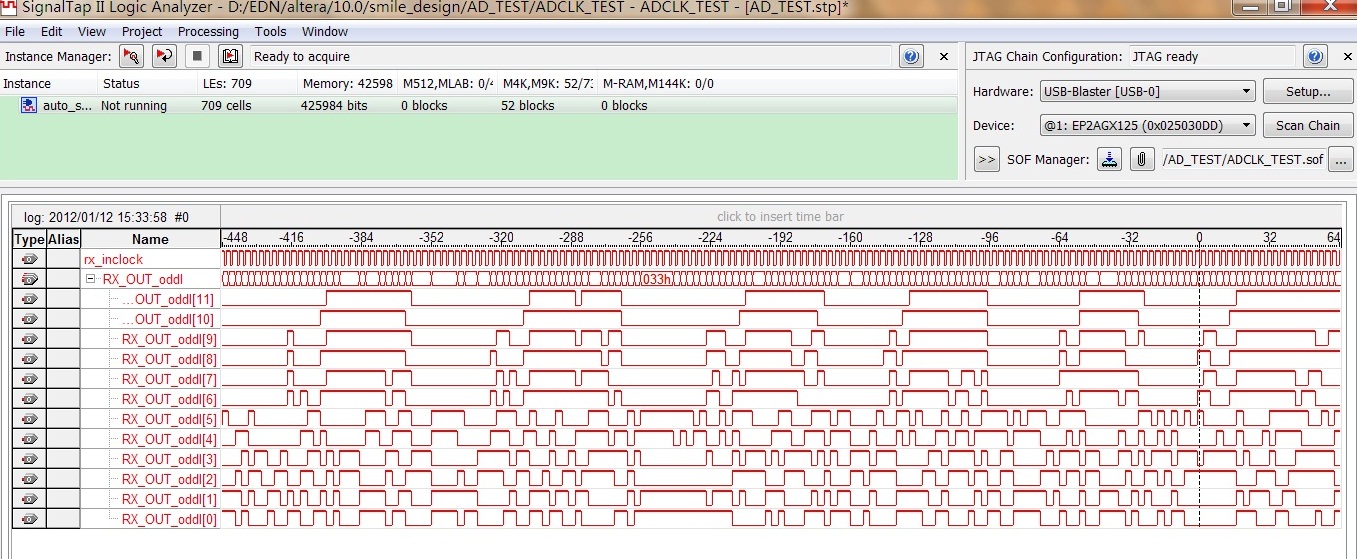
This is what I got from the DDR LVDS interface.RX_OUT_oddl[11:0] is the signals from the ADC's LVDS after the DDR_LVDS logic in the FPGA board.
I don't have the TSW1200, so I evaluate the ADC in my Altera ArriaII board.
All the configuration is default.
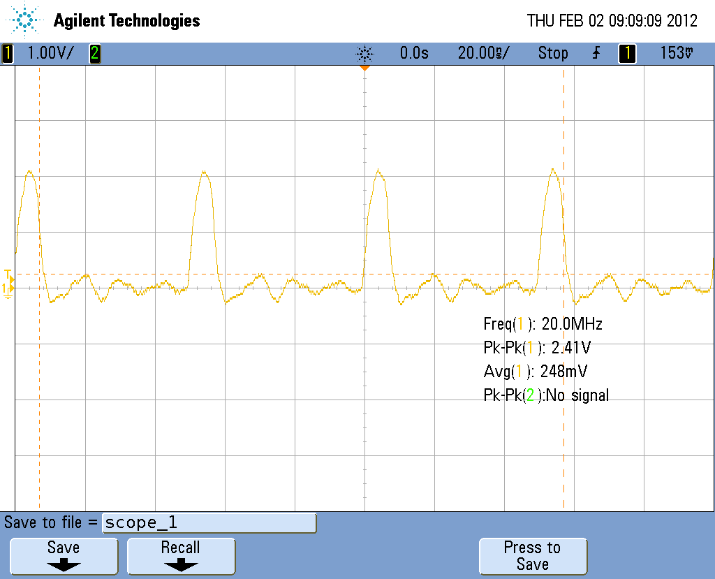
CLK of the ADC is a external 150MHz. (use option3. LVCPEL without 245.76MHz filter)
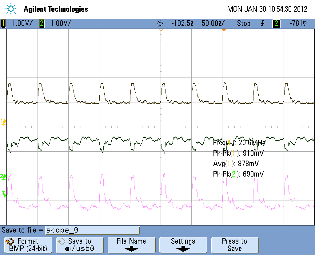
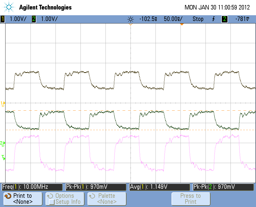
Input signal is a sine wave (Vpp = 1V, frequency = 200KHz, Voffset = V, 50om resistence signal output from a Function waveform generator)
More over, either the sine wave or square wave input ,the output is no different. All these output seems like a square wave(very likely the picture blow)
if I change the signal's input frequency or amplitude , the waveform changes as it should be. (SO the signal has been transmitted to the FPGA)
What's more, I change the SEN from LVDS 2's complement to LVDS binary offset. There is no difference between what I got from FPGA.
Can anyone help me to explain this ?
thank you
Alan


