This thread has been locked.

If you have a related question, please click the "Ask a related question" button in the top right corner. The newly created question will be automatically linked to this question.

DAC7760: CLARIFICATIONS ON DAC7760

Part Number: DAC7760
Other Parts Discussed in Thread: DAC8760EVM, TIPD153

Dear Sir, 

Can you please explain the following points :- 

  1. What is loop compliance Voltage , how to measure the same. 
  2. It has been mentioned that "AVSS TIED TO GND". Can you please elobrate which ground pin to be connected and procedure to connect the AVSS TO GND. 
  3. In the Voltage output - Load Conditions - You has ased us to add 4nf external compenstation capacitor. Can you porvide to which pins do we have to connect 
  4. You have mentioned DC OUTPUT IMPEDENCE  AS 0.3Ohms at CODE =0X8000- CAN you elborate on this. 
  5. What is the Iset Resistor has been menitioned by you as 15KOhm low drift resistor . Can you mention the part no. of specifciation of the Resistor. 
  6.  Where Shall we connect the VSENSE PIN TO VOUT . In our Cirucit We are having a diode to protect the Vout pin , if any voltage is applied to Vout pin. We have attached a circuit for your reference can you please suggest where to connect Vout pin
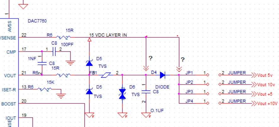
  7. Schematic.jpg
  8. What is the loop compliance voltage and how to mesure it.
  9. You have asked us to connect external compensation capacitor of 4nF. Where shall it be connected and what is the use.
  10. What is the maximum connectable load on Iout . RL for Iout.
  11. You have suggested 5Kohm to connect between Vout and Vsesne. Where as in the application circuit its 15 Ohms , which shall be used.
  12. We have Boost Circuit that is attached for your reference . Please confirm wether the circuit is correct or not.
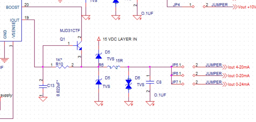
  13. Schematic1.jpg
  14. We have used MJD31CTF Transistor , please suggest if that is ok or do you recommend an alternate part.
  15. We are not using HART Communication , How shall we connect the Hart pin directly to ground or shall be left open.
  16. What shall be status of NC Pin. Shall it be left open or connected to ground.
  17. We are only connecting Vout and Vsense . I that scenario what shall be short circuit current limiting solution please confirm. The short circuit current limiting protection given in your application notes cannot be used as there are space constraints.
  • Hi,

    1. The compliance voltage is measured from the AVDD voltage to the output pin voltage. If your IOUT is 15mA with a 1kΩ load, theoretically, you would have an output of 15V. However, if the AVDD voltage is 15V, the output couldn't be at 15mA because the output FET would have a VDS of 0V, and the output device couldn't drive the total current. At the output you need a compliance voltage to be sure that the output drive is correct. In the DAC7760, this voltage is about 1.25V-1.5V for current output and is shown in Figure 7-70. The recommended operating conditions table on page 5 says this value is 2V maximum. For the voltage output mode, this voltage is the headroom voltage (and footroom voltage), which is 0.5V.

    2. I would consider all of the ground pins to be analog ground and connect those pins to AVSS using a ground plane. From the other E2E post, the example layout in the datasheet shows something similar.

    3. This 4nF is the capacitance at CMP to VOUT. The CMP node is a connection to the buffer amplifier. The added CCMP capacitance is a Miller capactance used for stability at higher VOUT capacitive loads.

    4. This is basically a measurement of the load regulation at the voltage output of the device when the output is at half scale.

    5. The RSET resistor is used to set the current of the DAC output based on Figure 8-3. Because this output current is set based on a voltage across a resistor, you want this resistance to be of high accuracy and low drift. Any error in this resistance reflects on the error on the output current. If your resistance is 0.1% high, then the output current will be 0.1% low. In the DACx760EVM, we have the Susumu RG1609P-153-B-T5 in the BOM, but you'll need to check to see if this is the right accuracy for you.

    6 and 7. I would not use D4 in series with the output. The problem is that the SENSE pin is a feedback to the output buffer. With a diode in series, the feedback works when there is load on the output. However, if there is no load, you lose the feedback because the amplifier cannot source current. I think you would have problems with the output drifting (I would guess at low voltage) if the diode is used. It might work if the diode is not in the feedback, but then you'd always have a 0.6V error in the output voltage.

    I would use an output similar to what we use in the EVM and in Figure 9-6 on page 49 in the data sheet. If you needed to increase the protection of the VOUT pin, I would increase the series resistance at VOUT.

    8. Answered in 1.

    9. Answered in 3.

    10. The maximum resistive load on IOUT is determined by the compliance voltage and the voltage from the maximum output current. First, the compliance voltage is 2V. If the supply is 15V, then the maximum voltage is 13V at the IOUT pin. In the 0-24mA range, the maximum current output is 24mA. With 13V at 24mA, the largest resistor you could use for a load would be 542Ω.

    11. You would use the 15Ω in all cases. The 5kΩ is placed in case the connection is broken. In many use cases, the output and sense lines run very far from the device. If these lines are accidentally broken, then the 5kΩ resistor prevents the output amplifier from becoming open loop. On the EVM, normally the VOUT and +VSENSE are connected. However, the 1kΩ R7 is used in case the sense line is broken.

    12 and 13. I think this boost circuit should work. It is similar to what is used in the EVM. I don't think the added circuitry will affect the operation of the device, just make sure the TVS diode has a low current leakage.

    14. The MJD31CTF should work fine. The DAC8760EVM uses a FZT651TA, which is a 60V, 3A NPN transistor, which is similar.

    15. If HART is not being used, there's no required connection to the HART-IN pin and it can be left floating. However, we generally recommend AC coupling the HART-in pin to ground with a capacitor to prevent EMC/EMI noise from coupling into the pin. One of our TI designs (TIPD153) uses a 22nF capacitor for the pin. The IEC61000-4-3 radiated immunity test at 20V/m did not produce any observable output disturbance.

    16. I would leave the NC pins unconnected. The DACx760EVM leaves these pins unconnected as well.

    17. The typical short circuit current limit for the VOUT is 30mA. It typically does not depend on the VSENSE connection. The short circuit value varies depending on the shorting voltage (to ground or other voltage) and temperature as shown in figure 7-44. What other short circuit current limiting solution did you see?

    If you haven't done so, I would look at the DACx760EVM to see how the board is constructed. If you are able to get one, it is a handy tool for evaluating the device.


    Joseph Wu