Dear TI Community,
I'm over a design using the octal DAC DAC8718. The status quo is:
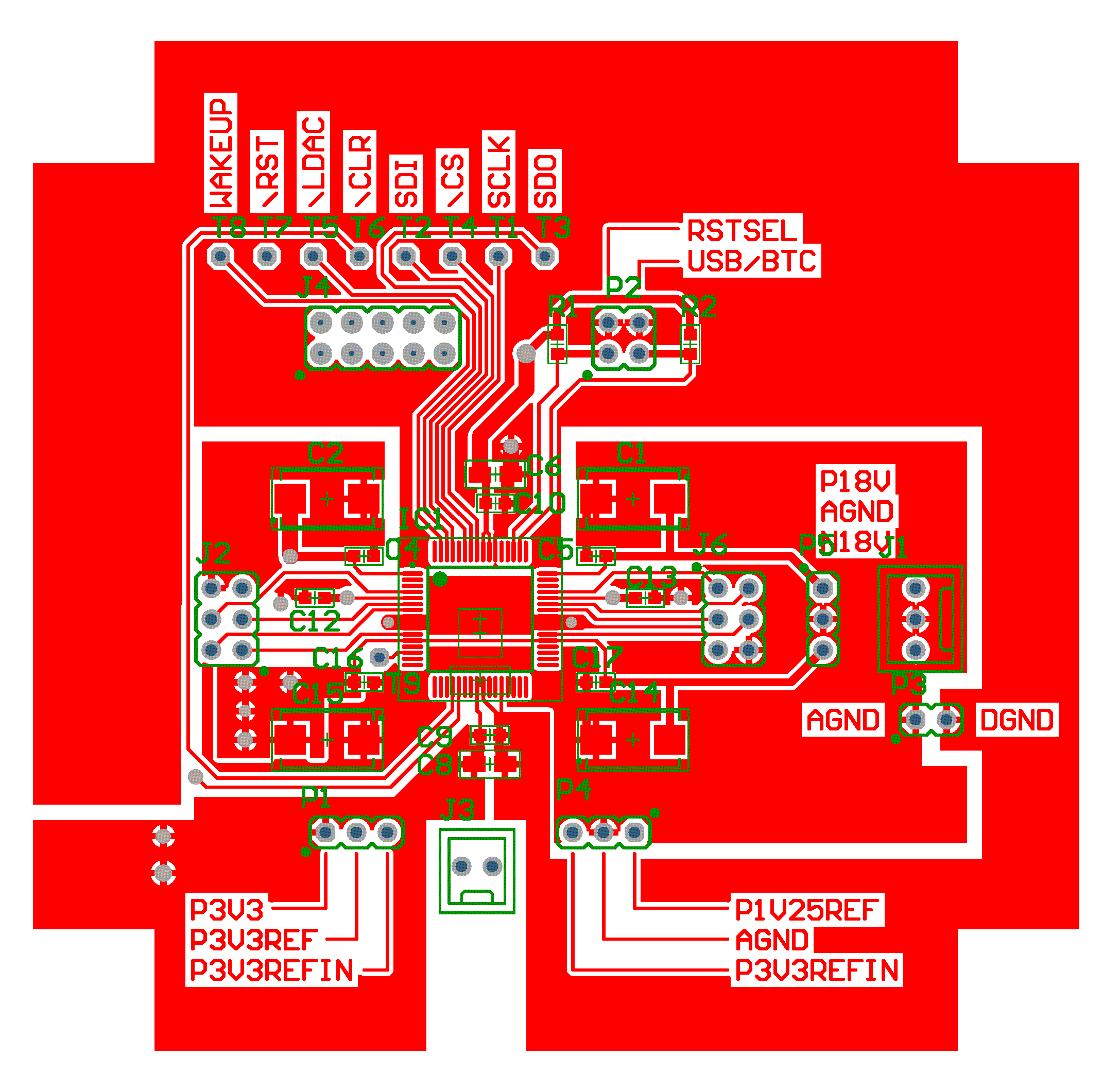
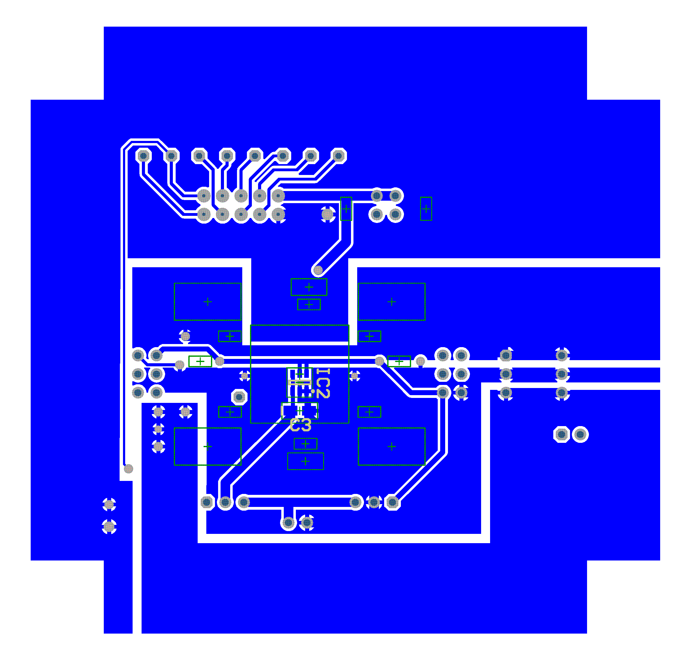
- The DAC is on a homebrewed double sided PCB completeley separated from the other digital circuit stuff
- This board is connected to the digital board using two iCoupler digital isolator chips sitting on a 3rd PCB
- The boards are connected with each other using 10 wire flat ribbon cables (length: approx. 10cm = 4")
- Supply voltages come out of two separate laboratory DC power supplys. One for the µC and other digital stuff as well as the µC side of the iCoupler isolator board, the other one supplies the DAC board as well as the DAC side of the iCoupler isolator board. The two power supplies don't have any ground or other connection with each other.
- I installed 33 ohms series resistors into the following lines: SCLK, SDI, \CS, \LDAC, SDO. Unfortunateley I didn't install them onto the DAC board, but onto the isolator board, so quite far away from the bus endpoint
- The configuration of the DAC is as follows: AVDD=+15V, AVSS=-15V, DVDD=IOVDD=3.3V, Vref=1.25V (REF3212), Gain = 6
- Supply Pins are decoupled as follows: 10µF||100n@AVDD&AVSS, 1µF||100n @DVDD&IOVDD, 100nF@REF-A&REF-B
- The DAC board uses split AGND and DGND ground planes connected near the DAC (<1cm=0.4")
Here's the schematic of the DAC Board:
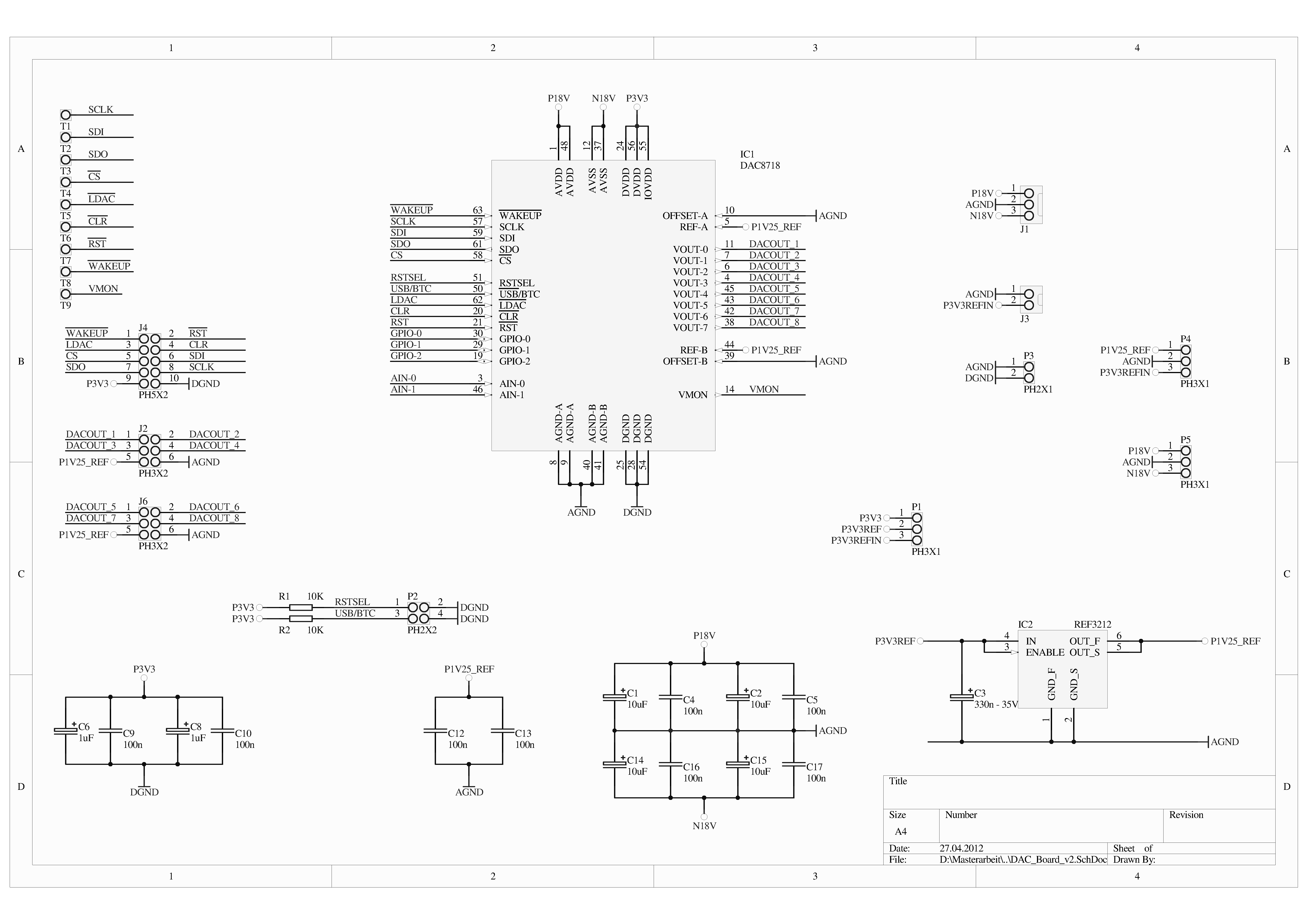
Figure 1: Schematic of the DAC board (click to enlarge)
OK, that are the priors, now the problems.
1. I have - in my opinion quite serious - SPI interference in my DAC output signal. Figures 2 to 4 illustrate this. See figure descriptions for further details. Can anybody please tell me what to do to get rid of this? Has anybody reached better performance?
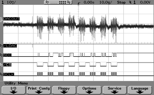
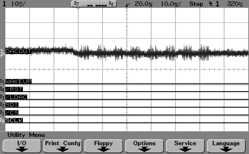
Figure 2: What you see is DACOUT3 as well as some digital control signals as descripted in the figure. DAC3 is performing a -16LSB step on the 4th rising edge of \CS. The code transition is from 0x7FC0 to 0x7FB0, which is near midscale (0V). As you can see, the DACOUT3 signal is quite serious corrupted by the SPI communication signals. Most prominent one is SCLK but also the \LDAC spike (which is currently not used but inserted for demonstration purposes) causes a spike in the output signal.
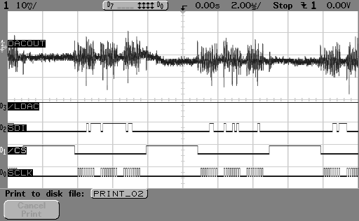
Figure 3: This is just a zoomed version of Figure 1 which shows clearly the relationship between the SPI signals and the 'noise' at the output.
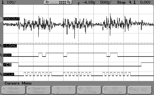
Figure 4: Another more zoomed version shows that the \CS signal causes an interference at the output, too.
Any suggestions for removing these spikes? I took care to route any high speed digital signal within the DGND plane. Supply cables are about 15cm = 6" in length. The output signals are measured with the probe connected directly to the pin header which is about 2.5cm = 1" away from the DAC. No load is connected to the DAC.
@TI staff: In the datasheet (all traces on p.24) I cannot see anything, which looks like SPI interference. You use a load consisting of 10kohms||240pF. If I do this the circuit begins to ring. Maybe you can test the circuit without any load and tell me about your results.
Ok, enough about SPI interference, let's come to the second problem, the settling time. In the datasheet (p.24) the DAC settles in about 14µs to less than 1LSB as a response on a full scale step and within about 10µs on a half scale step. Now have a look at my records (Figure 4 and 5)

Figure 5: This is a step of about -55mV which corresponds to a codestep of -480LSB. After the trigger (rising edge of \CS) the output settles down -3.5mV within 242µs. 1LSB is about 115µV. It looks like an exponential decay.
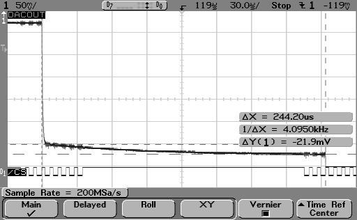
Figure 6: This is a step of about -275mV which corresponds to about -2400LSB (5x-480LSB). The decay is similar in duration but higher in amplitude. Seems to depend on the step amplitude.
By the way: You can see the SPI interference again in both figures, 5 and 6.
Hopefully anybody has an idea of solving any of these two problems. Both would be even better. Maybe there is even only one solution for both problems which would be the best case for me ;-). If you have further questions about the setup, don't hesitate to ask.
Best regards
Robert