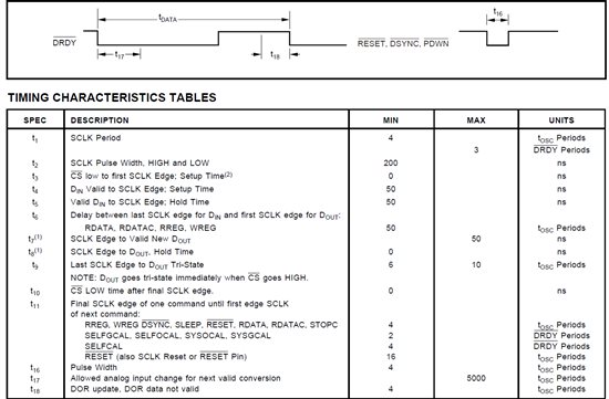
I read the posts on the ads1241 and while some of that made sense I'm still a little in the dark concerning the proper sequencing of commands to minimize settling time error.
Oscillator frequency is 4.9152 MHz
Configured for 15Hz operation
~DRDY is not wired to the processor. It’s value is read from the register.
Have an client with an existing design and they are having some intermittent problems with this device. I found a problem where they were not waiting the required 50 osc periods between the command and data phases on the register reads and ADC conversion read. So that is now working to specification.
After that, I wanted to look at the processes for programming the ADC to use all 8 channels. The current algorithm is
1. wait for ~DRDY to be true (0) by register read
2. read ADC conversion value
3. set next MUX channel
4. increment MUX channel (for next time through loop)
5. wait for 250 ms
6. go to step 1
What I noticed with this algorithm is that ~DRDY is always 0 when the register is read in step 1 because ~DRDY is only false(1) for 16ms or 32ms after the MUX channel is set. I looked at ~DRDY with an o-scope in conjunction with the SPI commands in the same trace to determine this relationship.
So here are my questions:
Why is ~DRDY false (1) for 16ms or 32 ms? It seems like this is the conversion time and I don’t understand why it’s variable. Usually the conversion time is fixed.
The data sheet specifies that you should change the MUX channel as quickly as possible once ~DRDY goes low or you will get settling errors. This is on page 10, figure 2 of the data sheet. This has me confused. Since setting the MUX channel causes ~DRDY to go false(1) then you would not be able to read the data from the previous conversion after the MUX change. So I need help here in determining if the above algorithm is correct or should be changed.


