Because of the Thanksgiving holiday in the U.S., TI E2E™ design support forum responses may be delayed from November 25 through December 2. Thank you for your patience.

This thread has been locked.

If you have a related question, please click the "Ask a related question" button in the top right corner. The newly created question will be automatically linked to this question.

TLC7226 data sheet?

Other Parts Discussed in Thread: TLC7226

Hello,

I would like to make a ramping voltage from approximately 0.3VDC up to approximately 1.0VDC.

To accomplish this I decided to try out the TLC7226C from TI. I was able to get this chip to ramp from 0 volts to any voltage up to 10V max. But now, I don't want to start from 0 volts DC. I would like to start from 0.3VDC and ramp up to 1.0 VDC.

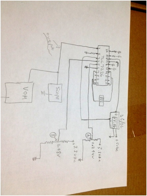
Please view diagram #1 below with circuit. Based on schematic, I have point "A" which when not connected to pin #5 of the TLC7226C part reads 0.294 VDC. But as soon 
as I connect point "A" to pin #5 of the TLC7226C, I read a voltage at pin#5 of .54volts DC. ??? Why?

Isn't pin#5 a high impedence input for the analogue ground... so why doesn't it read 0.294 VDC as intended by point "A"???


DIAGRAM#1:

Another problem I have is interpreting what the spec sheet is really saying... please consider the following!!!!

Still referring to the TLC7226 part and its spec sheet at:

http://www.ti.com/lit/ds/symlink/tlc7226.pdf

If you go to p.4 of the data sheet and look for:

ri(ref) Reference input resistance 2 kΩ min and 4 kΩ typical.

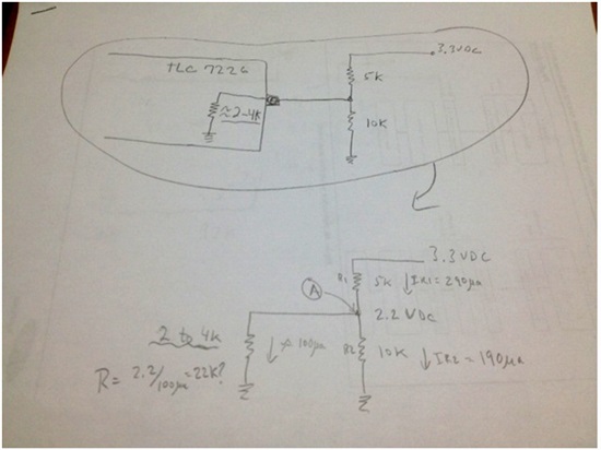
Questions in reference to diagram#2 below:

1) Does this mean that pin#4 of the TLC7226 part has a typical input resistance from 2kilo ohms to 4 kilo ohms?

2) Please refer to the attachment below where I tried to calculate the actual input resistance at pin #4. As a test, I have created a voltage divider to provide 2.2V as my reference voltage. I have measured the currents in the circuit. If I measure 2.2V at point "A", according to ohms law why is it that the calculation of the internal resistance comes out to 22K when the spec sheet says from 2 to 4 k???

DIAGRAM #2:

confused
All help very appreciated!


PS. I am trying to include attachments in my post but they won't show???

r

  • Hi RR,

    Ground pins cannot be high impedance because they close the current loop of the power supply. For example, if 1mA is consumed by a device, 1mA has to go back to the supply ground through ground pins.

    Since pin 5 is an analog ground pin, all the analog circuitry current (DAC and ref) is returned to the supply through this pin.

    Thus, resistors cannot be used to bias a ground pin because the supply return current will change the expected voltage. This will affect the device performance, and with very big resistors, the device will not power up.

    If a ground pin is not connected directly to the supply ground, a low impedance source like an op-amp or regulator should be used to sink or source the return currents while keeping a constant voltage.

    Regarding the reference impedance, it will also be affected by the resistors at AGND. Diagram#2 is not correct because it assumes that the reference pin ground is the digital ground. Since the reference pin is an analog input, its current should return to the supply by the AGND pin making the AGND its actual ground.

    Try calculating the reference impedance, with AGND and DGND connected at the supply ground. Also, make sure that there is a big capacitor bigger than 0.1uF at the reference pin to remove noise and avoid dynamic current effects. However, I recommend using an actual reference to drive the reference pin because normal resistors are very sensitive to temperature changes.

    Best regards,
    Rafael

  • Hello Rafael,

    Thank you for replying....

    >>>Ground pins cannot be high impedance because they close the current loop of the power supply. For example, if 1mA is consumed by a device, 1mA has to go back to the supply ground through ground pins.

    >>>Regarding the reference impedance, it will also be affected by the resistors at AGND. Diagram#2 is not correct because it assumes that the reference pin ground is the digital ground. Since the reference pin is an analog input, its current should return to the supply by the AGND pin making the AGND its actual ground.

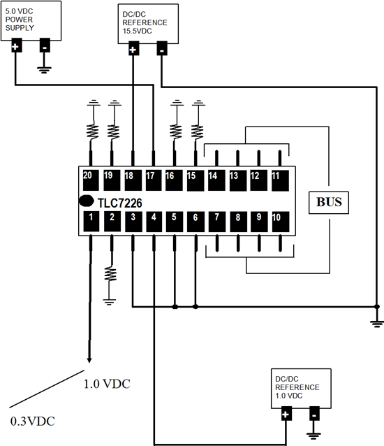
    I have put  pin#3, 5 and 6 to common ground this time and my reference pin#4 to 1.0 VDC. However this will ramp from 0VDC to 1VDC. How can I make it ramp  for example from 0.3VDC to 1VDC as in the diagram below.

    Basically where I am confused is how can we make the DAC start off at a positive offset voltage value without applying a less positive voltage on AGND? For example suppose I want an output range from 2 volts to 3 volts..... then 2volts at the AGND pin while ref pin is 3 volts or greater than 2volts will work . But you recommend that AGND should be simply tied to ground.. right? But on p.8 of the spec they show a diagram for bias for positive output mode and VI seems to be a positive voltage tied applied to AGND..... So how should the 7226 be wired when used in bias for positive mode?

    I don't use dacs very often! Any help would be very appreciated!

    please get back if you can!

    thanks 

  • Hi RR,

    You can use an op-amp to change the DAC output from 0 to 1 to 1 to 0.3V

    An op-amp was added to the diagram below to create the transfer function OUT = 1 – 0.7*DAC, where:

    If DAC = 0, op-amp output is 1V
    Or
    If DAC = 1, op-amp output is 0.3V

    Best regards,
    Rafael


  • hello Rafael,

    I thank you so much for your help. However I am a beginer

    in electronics and I am still learning transistors. Opamps is a little

    advanced for me. Using your solution would be like cheating

    because although your solution would work, I wouldn't know

    exactly what is really going on. So as I am learning transistors

    i would like to come up with a solution using transistors. 

    In any case I don't think I can have the 7226 ramp from 0.3VDC to

    1.0VDC usging the positive bias method on page 8 of the spec.

    I think the lowest ref voltage allowed by the part is 2V. so I am

    now looking into getting a 2.5VDC to 3.3VDC. with this ramp I will

    try to convert it to 0.3VDC to 1.0VDC so i can bias the base of

    a transistor and forth....

    in summary .... I am experimenting with all this stuff!

    thanks again

    r