This thread has been locked.

If you have a related question, please click the "Ask a related question" button in the top right corner. The newly created question will be automatically linked to this question.

About ADS8413..

I have some simple questions and report.

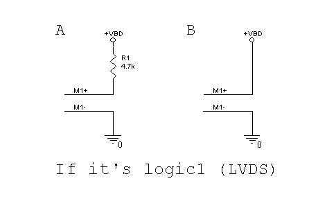
1. What exactly means that pulled up to +VBD in datasheet p#8, pin #30.

Is that figure like below? Which one is right?

2. Can I source CLK form Micro-Processor in the same way like pin #30 (related question #1)

3. In the document 'Using ADS8410/13 in Cascade Mode', Figure 3, Isn't the first ADC is a master according to LAT_Y/N connection. 

4. In the document 'Using ADS8410/13 in Cascade Mode', Figure 15. Shouldn't I connect ADC3 CLK_O to CLK_O bus?

  • Hi Will,

    Welcome to the TI E2E Forums!

    Regarding your questions:

    1. You can use a pull-up resistor less than 10 kOhm or have a direct connection to the digital supply. So, either pull-up connection will work.
    2. You can source an external CLK from a micro. The clock frequency must be around 200 MHz
    3. The master ADC is selected by the M1 logic setting (pins 30 & 31) and this ADC will output CLK_O on the common clock bus. The LAT_Y/N connection selects the first ADC which will output data on the SDO bus.
    4. Yes, if you are using an external clock source. If you use the internal clock of ADC3 as the synchronized clock source, then this connection is not connected to the common clock bus, but instead routed to the clock inputs of all the ADCs. Refer to figure 2 in "Using ADS8410/13 in Cascade Mode" for an internal clock configuration and figure 3 for an external clock configuration.

    NOTE: There are a few minor issues in figures 2 & 3 in the above reference document: The "LOGIC 1" text in figure 2 was not displayed properly in the PDF. It refers to setting M1 of ADC 2 high to configure ADC 2 as the master. Also, both figures 2 & 3 have some outputs connecting to the wrong bus. However, the general idea is conveyed that outputs (SDO, CLK_O, and SYNC_O connect to their respective common bus, except for the CLK_O of the ADC that is providing the synchronized clock input for the rest of the ADCs.

    Best regards,
    Chris

  • Thank you for your reply.

    Regarding external CLK, We were planing to source a few different value of clock.

    Does it have to be around 200Mhz? Is it impossible to operate low rate such as 100M or under?